
Hardmask materials

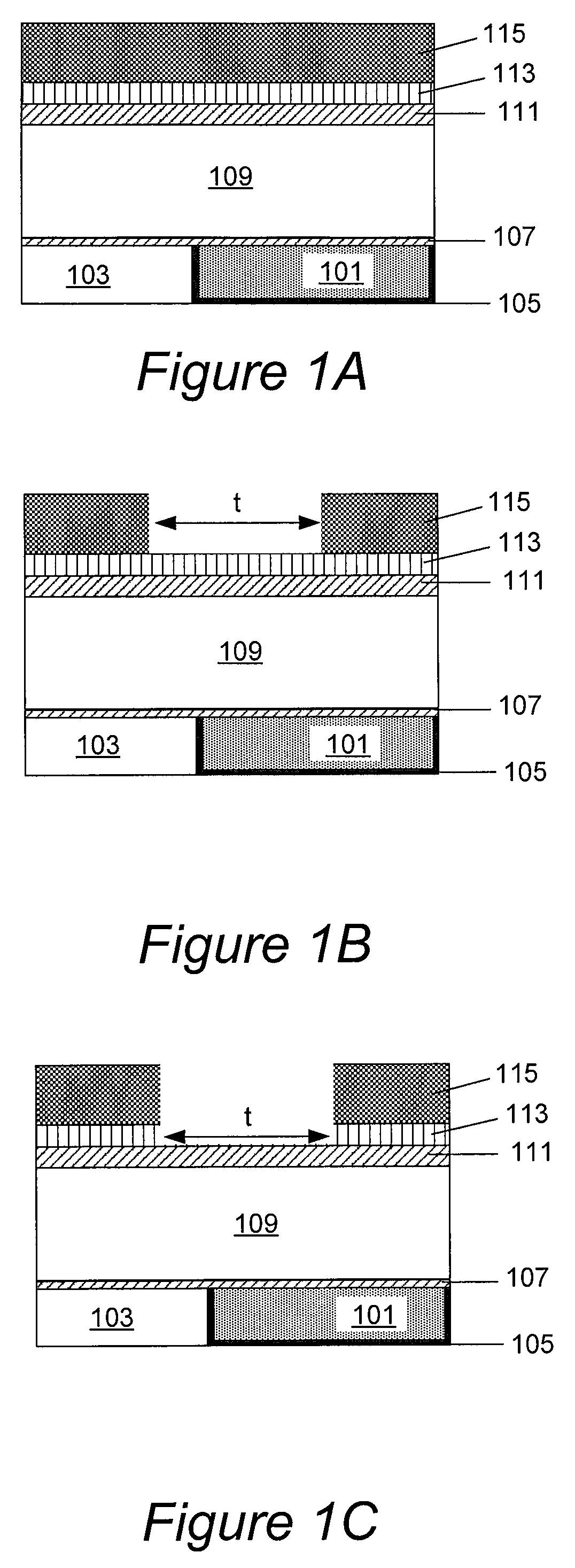
a technology of hardmask and material, applied in the field of hardmask films, can solve the problems of poor alignment, low stress and high hardness (or high modulus) are especially difficult to achieve, and achieve low stress, high hardness and/or young's modulus, and poor pattern alignment in lithography

Active Publication Date: 2012-08-21
NOVELLUS SYSTEMS
View PDF73 Cites 19 Cited by
  • Summary
  • Abstract
  • Description
  • Claims
  • Application Information

AI Technical Summary

Benefits of technology

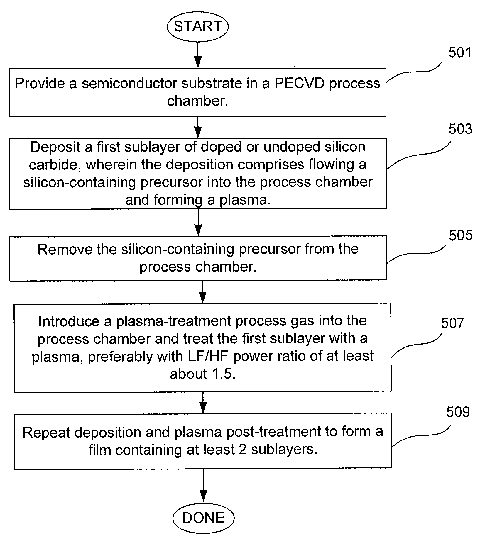
The patent describes a method for making a hardmask film with low stress and high hardness for use in semiconductor processing applications. The method involves depositing a multi-layer silicon carbide film using plasma enhanced chemical vapor deposition (PECVD) and plasma treatment to increase hardness and decrease stress. The resulting film has high content of Si—C bonding and a density of at least about 2 g / cm3. The method can be used with a variety of silicon carbide films, such as doped or undoped silicon carbide films, and boron-containing films. The resulting film has improved properties and can better align and protect the underlying material during lithographic processes.

Problems solved by technology

In lithographic applications, hardmask materials with low stress are needed because materials with highly compressive or tensile stresses lead to buckling or delamination of the hardmask film on the substrate, and, consequently, to poor pattern alignment in lithography.
This combination of low stress and high hardness (or high modulus) is especially difficult to achieve, as harder materials typically possess higher compressive stress.
The use of such highly-compressive hardmask, particularly with soft ultra low-k dielectrics (k=2.8 and less), and particularly to define higher aspect ratio features (e.g., features with aspect ratio of 2:1 and higher), leads to poor alignment, and to undesired wiggling of the formed structures.

Method used


Image

  • Hardmask materials
  • Hardmask materials
  • Hardmask materials

Examples


Embodiment Construction

Introduction and Overview

[0033]Hardmask films for back-end and front-end semiconductor processing applications are provided. The films comprise materials selected from the group consisting of SiCx (doped or undoped), SixByCz, SixByNz, SixByCzNw, BxNy, BxCy and GeNx.

[0034]The materials consist essentially of the elements that are recited in the corresponding formulas and optionally include hydrogen which is not explicitly recited. The subscripts x, y, z, and w indicate that the materials are not necessarily stoichiometric. The materials include dopants only if presence of dopants is explicitly mentioned. For example, undoped SiCx (silicon carbide) described herein is a material which consists essentially of silicon and carbon (not necessarily in stoichiometric proportions) and optionally includes hydrogen. Doped SiCx further includes a dopant element, such as boron, oxygen, phosphorus, or nitrogen.

[0035]In some embodiments materials provided herein have one or more of the following a...


PUM


Abstract

Hardmask films having high hardness and low stress are provided. In some embodiments a film has a stress of between about −600 MPa and 600 MPa and hardness of at least about 12 GPa. In some embodiments, a hardmask film is prepared by depositing multiple sub-layers of doped or undoped silicon carbide using multiple densifying plasma post-treatments in a PECVD process chamber. In some embodiments, a hardmask film includes a high-hardness boron-containing film selected from the group consisting of SixByCz, SixByNz, SixByCzNw, BxCy, and BxNy. In some embodiments, a hardmask film includes a germanium-rich GeNx material comprising at least about 60 atomic % of germanium. These hardmasks can be used in a number of back-end and front-end processing schemes in integrated circuit fabrication.

Description

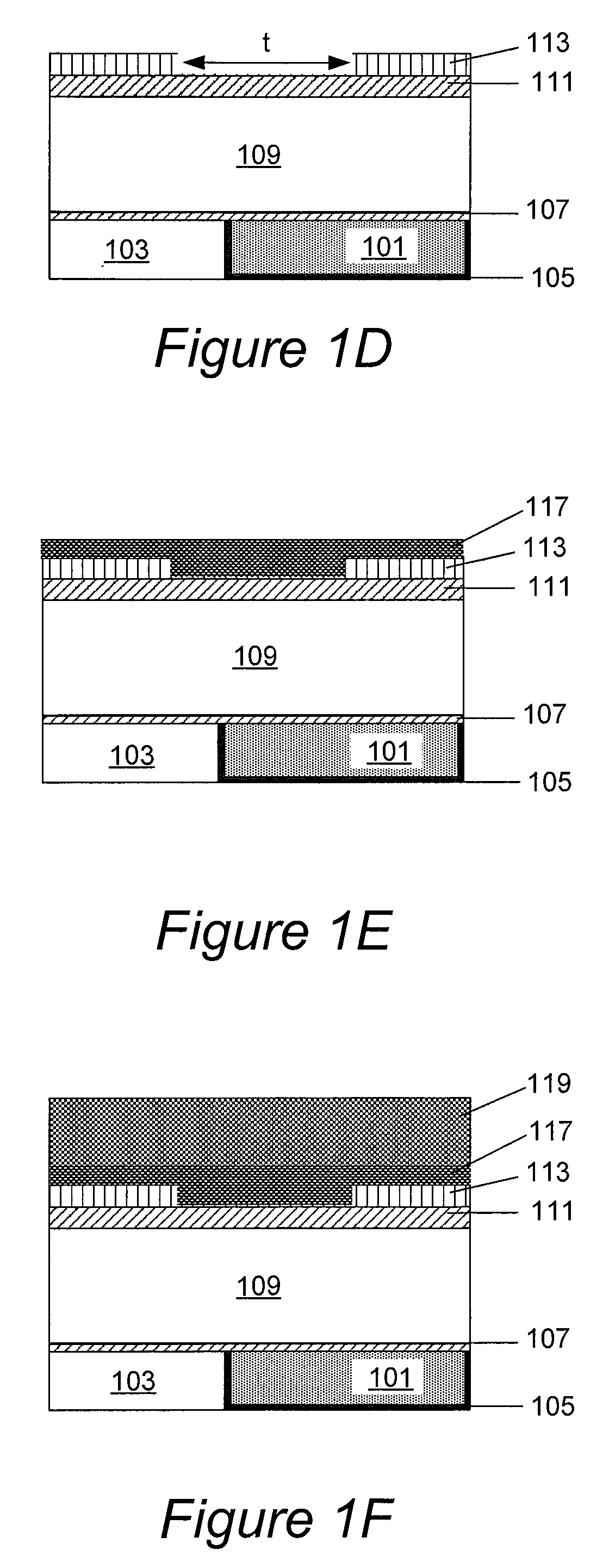
FIELD OF THE INVENTION[0001]This invention relates to hardmask films for use in semiconductor processing. The invention also relates to methods and apparatus for forming such films.BACKGROUND OF THE INVENTION[0002]Hardmask films are commonly used as sacrificial layers during lithographic patterning, e.g., during trench and / or via formation in a Damascene process. In Damascene processing, hardmask film is typically deposited onto a layer of dielectric that needs to be patterned. A layer of photoresist is deposited over the hardmask film (with an optional antireflective layer deposited between the hardmask and the photoresist), and the photoresist is patterned as desired. The lasers are typically used for alignment of the pattern with the underlying structures, and, hence, the hardmasks should be substantially transparent at the wavelengths used for alignment. After the photoresist is developed, the exposed hardmask film below the pattern is removed, and the exposed dielectric is etch...

Claims


Application Information

Patent Timeline
Patent Type & Authority Patents(United States)
IPC IPC(8): H01L21/311H01L21/461H01L21/469
CPCC23C16/30C23C16/34C23C16/505C23C16/56H01J37/32091H01J37/32165H01L21/02112H01L21/02167H01L21/022H01L21/02274H01L21/0332H01L21/31144H01L21/3148H01L21/318H01L21/32139H01L21/76813H01L21/67017C23C16/325Y10S438/942Y10S438/932
Inventor RANGARAJAN, VISHWANATHANANTONELLI, GEORGE ANDREWBANERJI, ANANDAVAN SCHRAVENDIJK, BART
Owner NOVELLUS SYSTEMS
Learn More