Hardmask materials

a technology of hardmask and material, applied in the field of hardmask films, can solve the problems of poor alignment, low stress and high hardness (or high modulus) are especially difficult to achieve, and achieve low stress, high hardness and/or young's modulus, and poor pattern alignment in lithography

a technology of hardmask and material, applied in the field of hardmask films, can solve the problems of poor alignment, low stress and high hardness (or high modulus) are especially difficult to achieve, and achieve low stress, high hardness and/or young's modulus, and poor pattern alignment in lithography

US20110135557A1Active Publication Date: 2011-06-09NOVELLUS SYSTEMS

Image

  • Hardmask materials
  • Hardmask materials
  • Hardmask materials

Examples


Embodiment Construction

Introduction and Overview

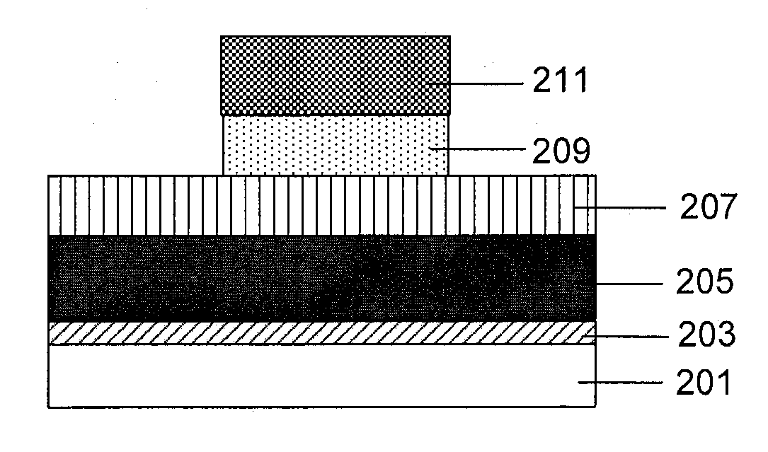
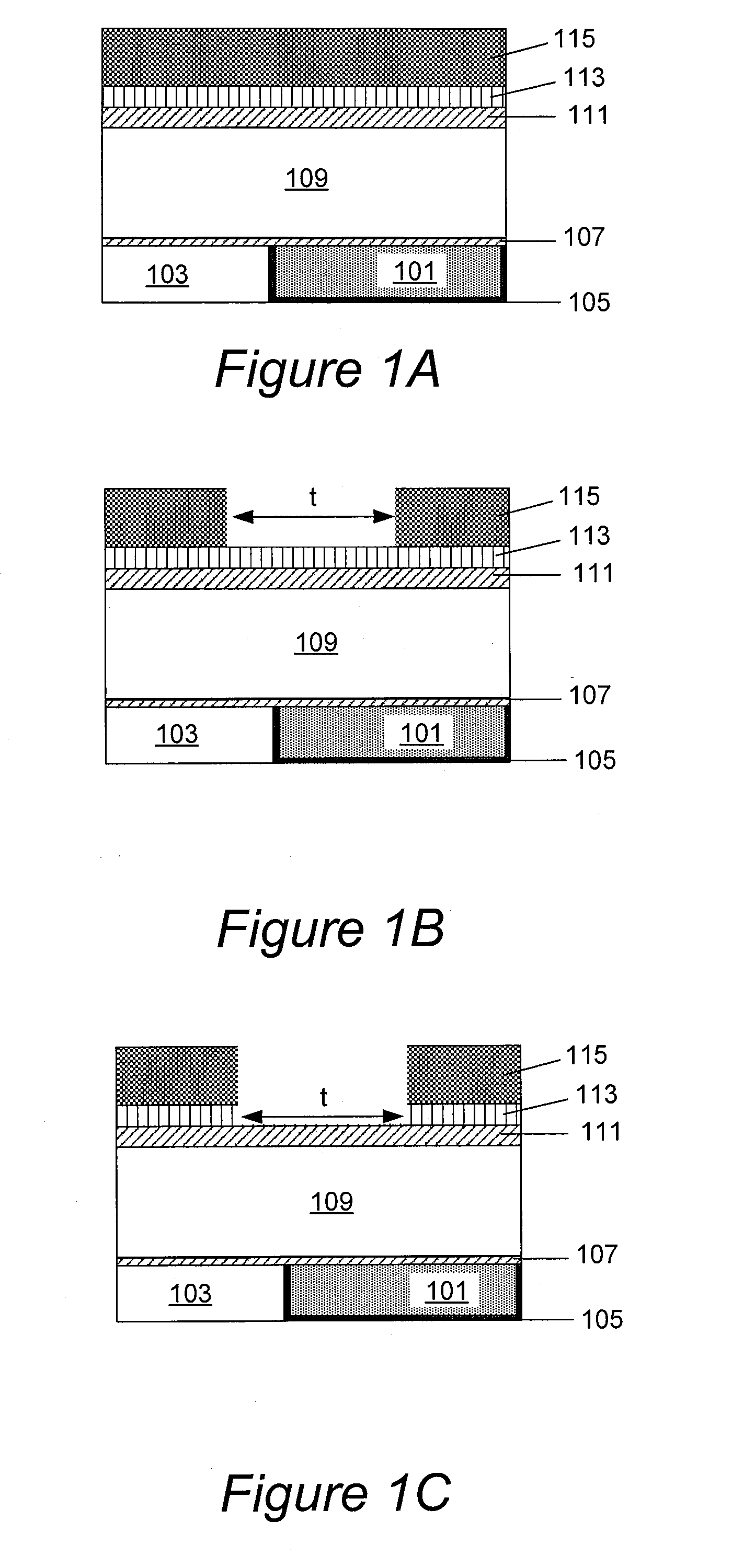
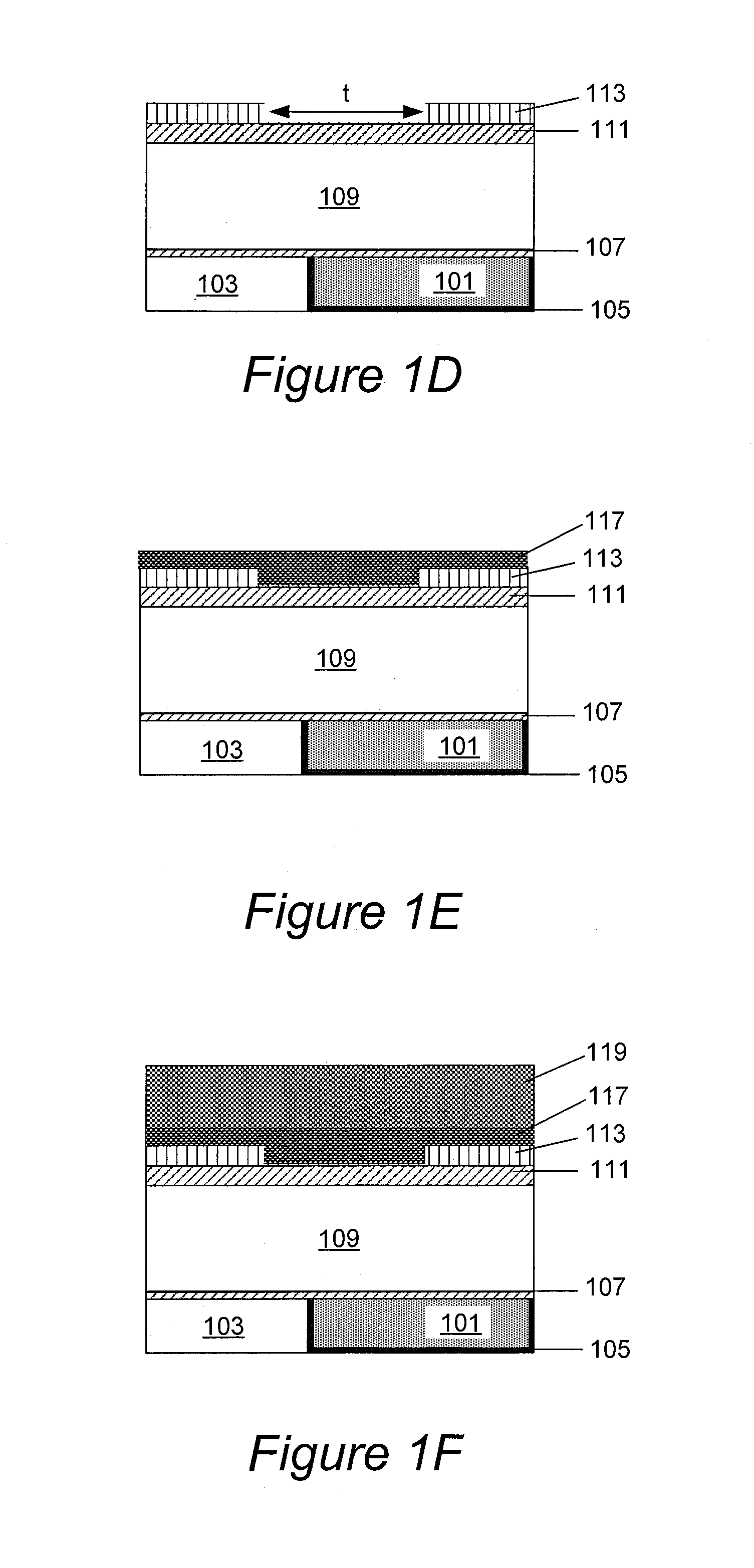
[0033]Hardmask films for back-end and front-end semiconductor processing applications are provided. The films comprise materials selected from the group consisting of SiCx (doped or undoped), SixByCz, SixByNz, SixByCzNw, BxNy, BxCy and GeNx.

[0034]The materials consist essentially of the elements that are recited in the corresponding formulas and optionally include hydrogen which is not explicitly recited. The subscripts x, y, z, and w indicate that the materials are not necessarily stoichiometric. The materials include dopants only if presence of dopants is explicitly mentioned. For example, undoped SiCx (silicon carbide) described herein is a material which consists essentially of silicon and carbon (not necessarily in stoichiometric proportions) and optionally includes hydrogen. Doped SiCx further includes a dopant element, such as boron, oxygen, phosphorus, or nitrogen.

[0035]In some embodiments materials provided herein have one or more of the following a...


PUM

PropertyMeasurementUnit
densityaaaaaaaaaa
dielectric constantaaaaaaaaaa
temperatureaaaaaaaaaa

Abstract

Hardmask films having high hardness and low stress are provided. In some embodiments a film has a stress of between about −600 MPa and 600 MPa and hardness of at least about 12 GPa. In some embodiments, a hardmask film is prepared by depositing multiple sub-layers of doped or undoped silicon carbide using multiple densifying plasma post-treatments in a PECVD process chamber. In some embodiments, a hardmask film includes a high-hardness boron-containing film selected from the group consisting of SixByCz, SixByNz, SixByCzNw, BxCy, and BxNy. In some embodiments, a hardmask film includes a germanium-rich GeNx material comprising at least about 60 atomic % of germanium. These hardmasks can be used in a number of back-end and front-end processing schemes in integrated circuit fabrication.

Description

FIELD OF THE INVENTION[0001]This invention relates to hardmask films for use in semiconductor processing. The invention also relates to methods and apparatus for forming such films.BACKGROUND OF THE INVENTION[0002]Hardmask films are commonly used as sacrificial layers during lithographic patterning, e.g., during trench and / or via formation in a Damascene process. In Damascene processing, hardmask film is typically deposited onto a layer of dielectric that needs to be patterned. A layer of photoresist is deposited over the hardmask film (with an optional antireflective layer deposited between the hardmask and the photoresist), and the photoresist is patterned as desired. The lasers are typically used for alignment of the pattern with the underlying structures, and, hence, the hardmasks should be substantially transparent at the wavelengths used for alignment. After the photoresist is developed, the exposed hardmask film below the pattern is removed, and the exposed dielectric is etch...

Claims


Application Information

Patent Timeline
09 Jun 2011
Publication
US20110135557A1
IPC
H01L21/31; C01B31/36
CPC
C23C16/30; Y10S438/942; C23C16/34; C23C16/505; C23C16/56; H01J37/32091; H01J37/32165; H01L21/02112
Inventors
RANGARAJAN, VISHWANATHAN; ANTONELLI, GEORGE ANDREW