Semiconductor device manufacturing method

a semiconductor and manufacturing method technology, applied in the direction of semiconductor devices, basic electric elements, electrical appliances, etc., can solve the problems of increasing threshold current, increasing power dissipation, and reducing internal quantum efficiency, so as to reduce the complexity of the device fabrication process, reduce the resistance, and reduce the resistance

Inactive Publication Date: 2012-09-18
PANASONIC CORP
View PDF20 Cites 4 Cited by
  • Summary
  • Abstract
  • Description
  • Claims
  • Application Information

AI Technical Summary

Benefits of technology

[0022]According to the present invention, a p-type gallium nitride-based compound semiconductor layer is cooled with the supply of hydrogen gas to a reaction chamber cut off, thereby making the concentration of hydrogen in the reaction chamber during the cooling process lower than in a conventional process. As a result, the hydrogen atoms that have bonded to a p-type dopant while the p-type gallium nitride-based compound semiconductor layer is being formed can detach themselves easily from the p-type dopant during the cooling process. Consequently, the p-type dopant gets activated and the p-type gallium nitride-based compound semiconductor layer comes to have lower resistivity. According to the present invention, low resistivity that is required for a semiconductor device is realized even without performing an annealing process, thus reducing the complexity of the device fabrication process and cutting down the manufacturing cost significantly.
[0023]On top of that, since the annealing process can be omitted according to the present invention, surface roughening can be avoided. Such surface roughening never happens in a c-plane-growing p-type gallium nitride-based compound semiconductor layer that has been, and is still, used extensively. That is why it is particularly beneficial to the process of forming a p-type gallium nitride-based compound semiconductor layer, of which the crystal-growing surface is an m plane, to omit the annealing process.

Problems solved by technology

Consequently, the internal quantum efficiency decreases, thus increasing the threshold current in a semiconductor laser diode and increasing the power dissipation and decreasing the luminous efficacy in an LED.

Method used


Image

  • Semiconductor device manufacturing method
  • Semiconductor device manufacturing method
  • Semiconductor device manufacturing method

Examples


embodiment

(Embodiment)

[0041]A method for fabricating a semiconductor device according to the present invention will now be described with reference to the accompanying drawings. FIG. 6 is a flowchart showing a manufacturing process according to a preferred embodiment of the present invention and a conventional manufacturing process. Specifically, in FIG. 6, the flow of the manufacturing process of this preferred embodiment is indicated by the solid arrows, while the typical flow of the conventional manufacturing process is indicated by the dashed arrows.

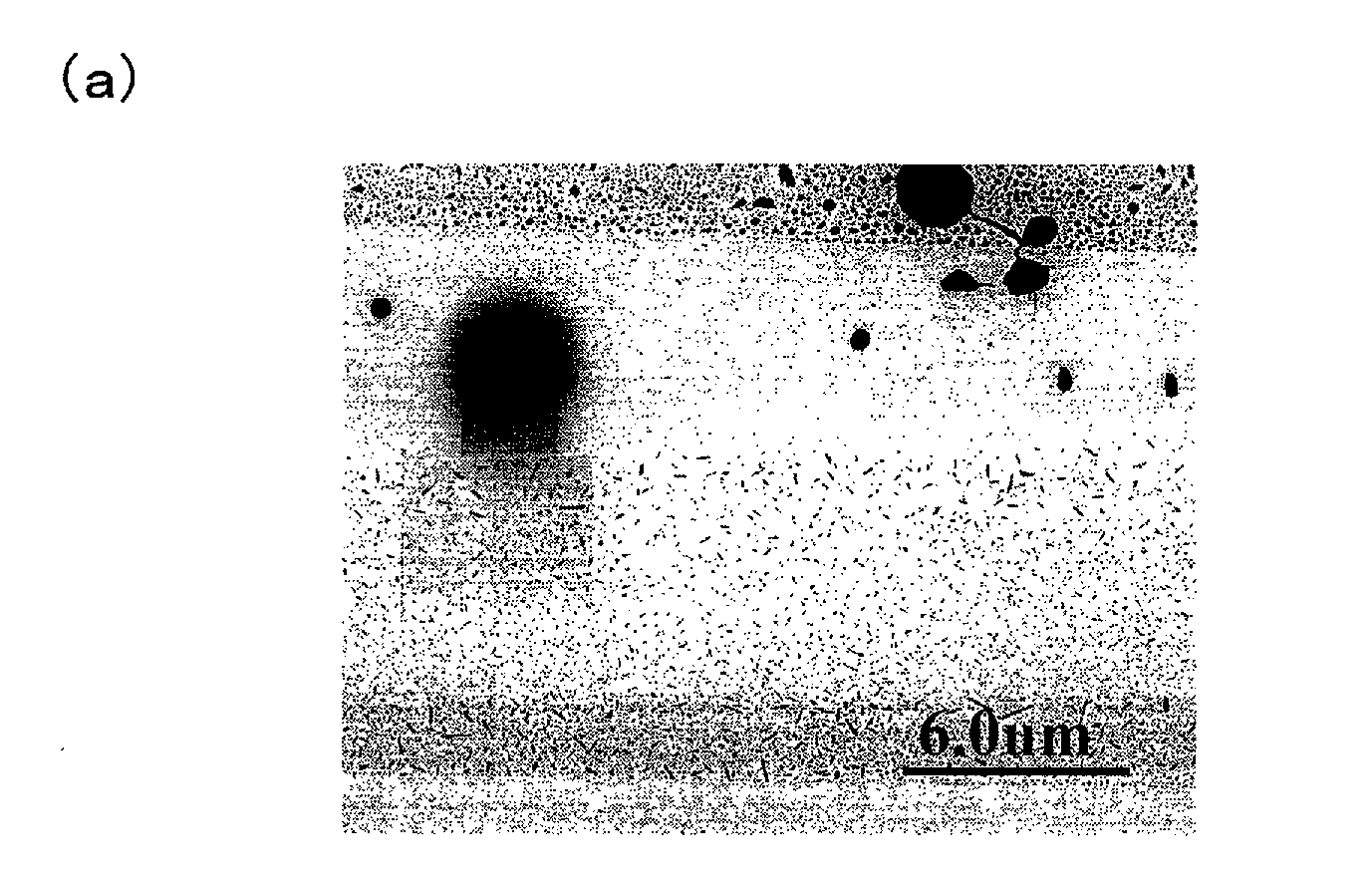
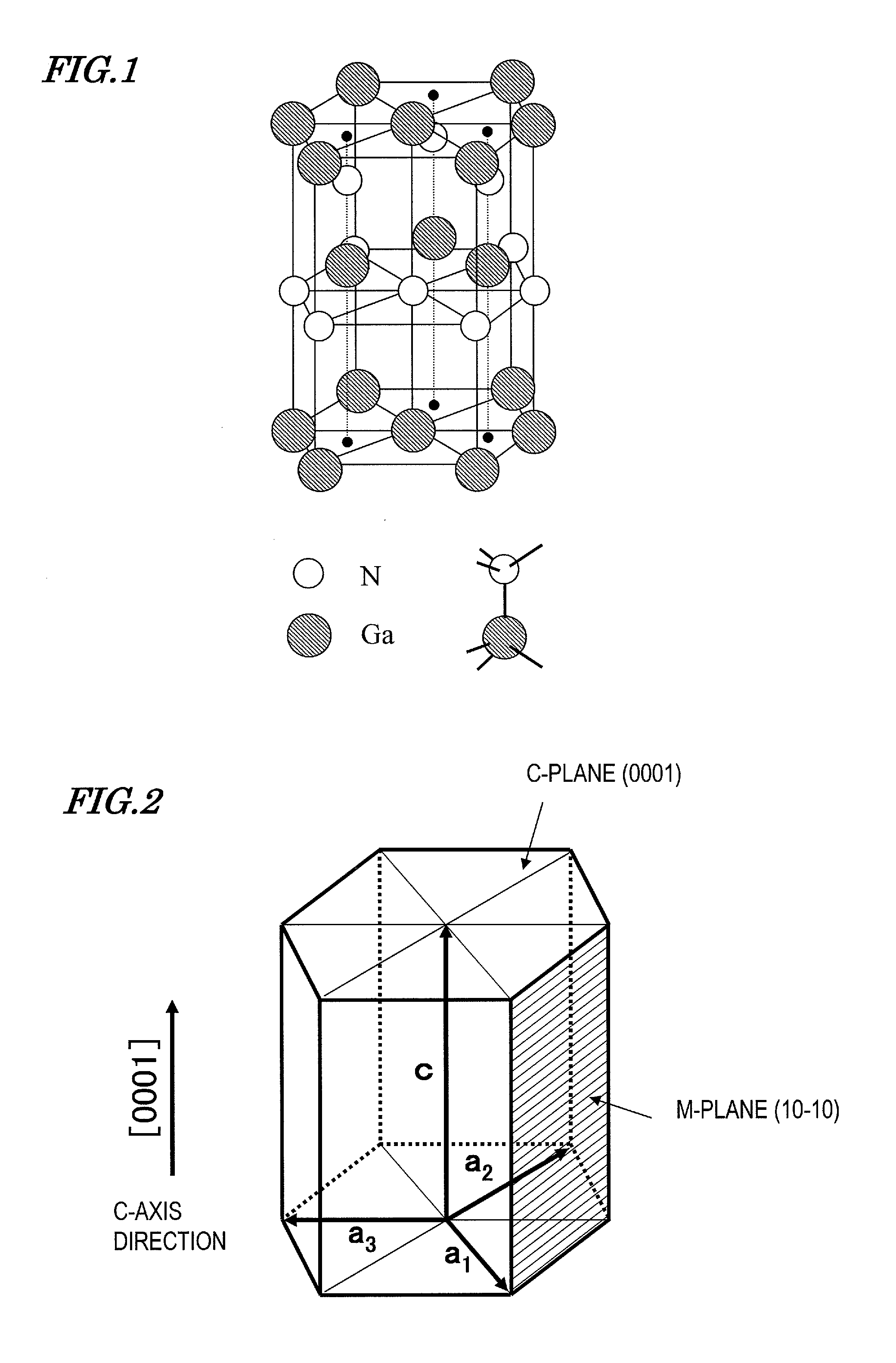
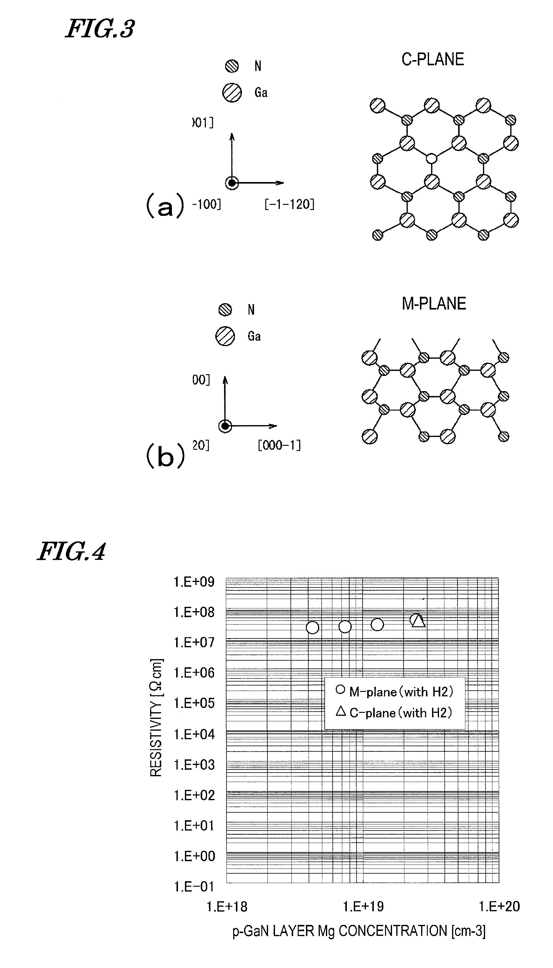
[0042]As shown in FIG. 6, in the semiconductor device manufacturing process of this preferred embodiment, the wafer is washed in Step S11 and then subjected to thermal cleaning in Step S12. Next, in Step S13, crystals of an m-plane-growing semiconductor layer are grown on the wafer by performing a metalorganic chemical vapor deposition process in a heated atmosphere. In this process, the actual m-planes do not have to be perfectly parallel to ...


PUM

PropertyMeasurementUnit
thicknessaaaaaaaaaa
temperatureaaaaaaaaaa

Abstract

A method for fabricating a semiconductor device according to the present invention includes the steps of: growing a p-type gallium nitride-based compound semiconductor layer by performing a metalorganic chemical vapor deposition process in a heated atmosphere so that the crystal-growing plane of the semiconductor layer is an m plane (Step S13); and cooling the p-type gallium nitride-based compound semiconductor layer (Step S14) after the step of growing has been carried out. The step of growing includes supplying hydrogen gas to a reaction chamber in which the p-type gallium nitride-based compound semiconductor layer is grown. The step of cooling includes cooling the p-type gallium nitride-based compound semiconductor layer with the supply of the hydrogen gas to the reaction chamber cut off.

Description

TECHNICAL FIELD[0001]The present invention relates to a method for fabricating a semiconductor device with a p-type gallium nitride-based compound semiconductor layer.BACKGROUND ART[0002]A nitride semiconductor including nitrogen (N) as a Group V element is a prime candidate for a material to make a short-wave light-emitting device because its bandgap is sufficiently wide. Among other things, gallium nitride-based compound semiconductors (which will be referred to herein as “GaN-based semiconductors” and which are represented by the formula AlxGayInzN (where 0≦x, y, z≦1 and x+y+z=1)) have been researched and developed particularly extensively. As a result, blue-ray-emitting light-emitting diodes (LEDs), green-ray-emitting LEDs and semiconductor laser diodes made of GaN-based semiconductors have already been used in actual products.[0003]A GaN-based semiconductor has a wurtzite crystal structure. FIG. 1 schematically illustrates a unit cell of GaN. In an AlxGayInzN (where 0≦x, y, z≦1...

Claims


Application Information

Patent Timeline
Patent Type & Authority Patents(United States)
IPC IPC(8): H01L21/203
CPCH01L21/02378H01L21/02389H01L21/0242H01L21/0254H01L21/02579H01L21/02609H01L21/0262H01L33/007H01L33/0095H01L33/16H01L33/32
Inventor KATO, RYOUFUJIKANE, MASAKIINOUE, AKIRAYAMADA, ATSUSHIYOKOGAWA, TOSHIYA
Owner PANASONIC CORP
Why Eureka
Try Eureka