Methods and apparatus for SRAM bit cell with low standby current, low supply voltage and high speed

a sram bit cell and low standby current technology, applied in the field of sram memory bit cells, can solve the problems of difficult to reliably do 6t storage cells, require a bit of control circuitry, and the dram circuit has relatively slow access time for reads and writes, etc., to achieve stable data storage, low standby current, and fast read

Active Publication Date: 2012-10-23
TAIWAN SEMICON MFG CO LTD
View PDF2 Cites 78 Cited by
  • Summary
  • Abstract
  • Description
  • Claims
  • Application Information

AI Technical Summary

Benefits of technology

[0017]These and other problems are generally solved or circumvented, and technical advantages are generally achieved by embodiments of the present invention, which provides in exemplary embodiments an SRAM bit cell with thicker gate oxides in the storage cell transistors and thinner gate oxides in the read port transistors. The use of the thicker gate oxides in the storage cell transistors provides a stable storage of data, and lower standby current. The use of the thinner gate oxides in the read port transistors provides fast read accesses and allows a lower Vcc,min. The power supplied to the read port may be coupled to a logic portion of the device, while the power to the storage cell transistors may be higher for improved reliability. The methods are arranged to form the dual gate oxide thickness SRAM cells with process steps that are compatible with the existing process flows used in semiconductor manufacturing.

Problems solved by technology

DRAM cells may be provided in very dense arrays, since a DRAM cell requires only a single access transistor and a storage capacitor; however, DRAM circuits have relatively slow access time for reads and writes, and require somewhat complicated control circuitry, and each DRAM cell stores data as charge on a leaky capacitor, so that the DRAM array must be refreshed periodically to maintain state.
This is difficult to do reliably for the 6T storage cells, however, due to process variations and other constraints increasingly imposed by shrinking device sizes and process advances.
Further, as semiconductor processes continue to advance, device sizes continue to shrink.

Method used


Image

  • Methods and apparatus for SRAM bit cell with low standby current, low supply voltage and high speed
  • Methods and apparatus for SRAM bit cell with low standby current, low supply voltage and high speed
  • Methods and apparatus for SRAM bit cell with low standby current, low supply voltage and high speed

Examples


Embodiment Construction

[0043]The making and using of the presently preferred embodiments are discussed in detail below. It should be appreciated, however, that the present invention provides many applicable inventive concepts that can be embodied in a wide variety of specific contexts. The specific embodiments discussed are merely illustrative of specific ways to make and use the invention, and do not limit the scope of the invention.

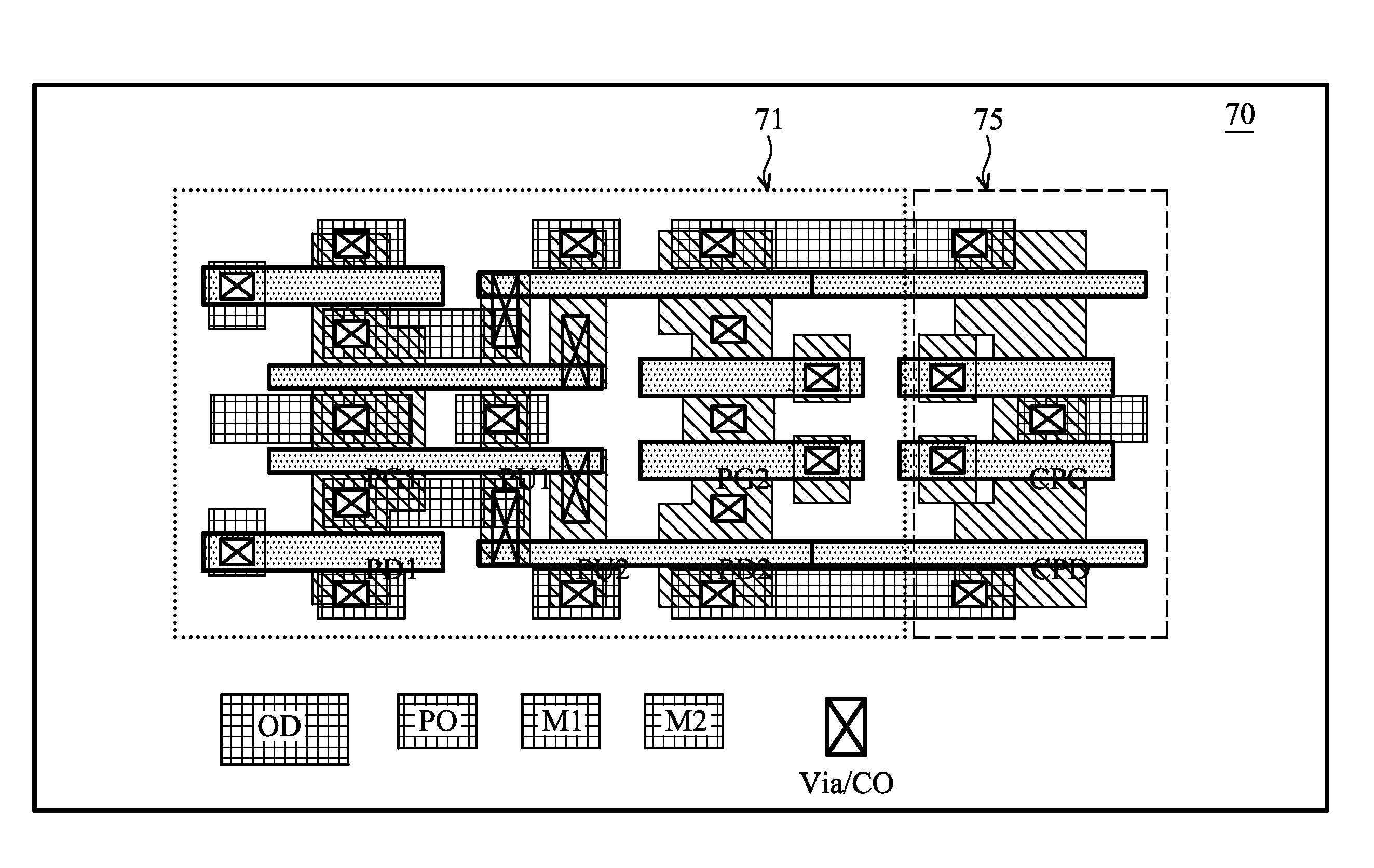
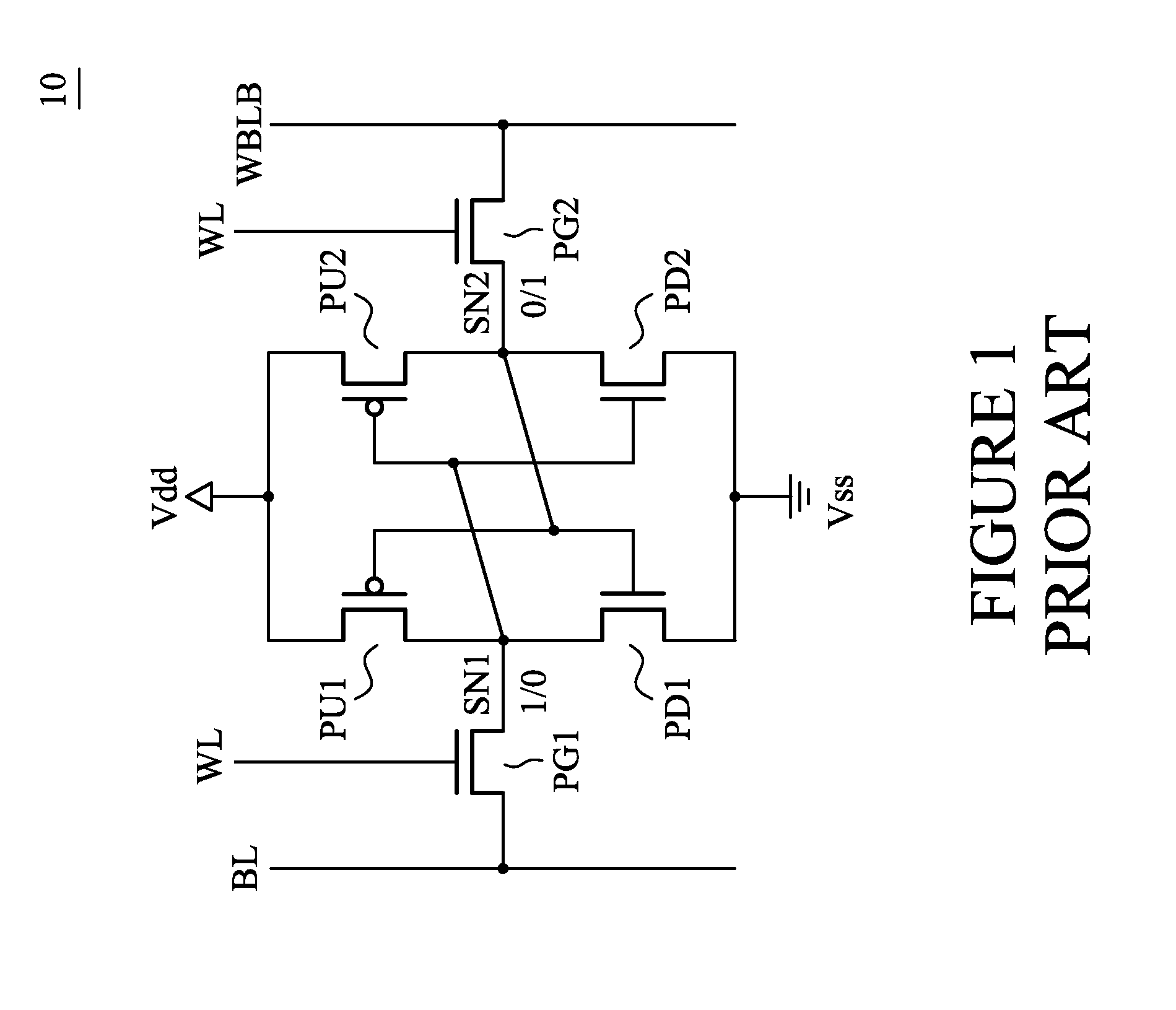
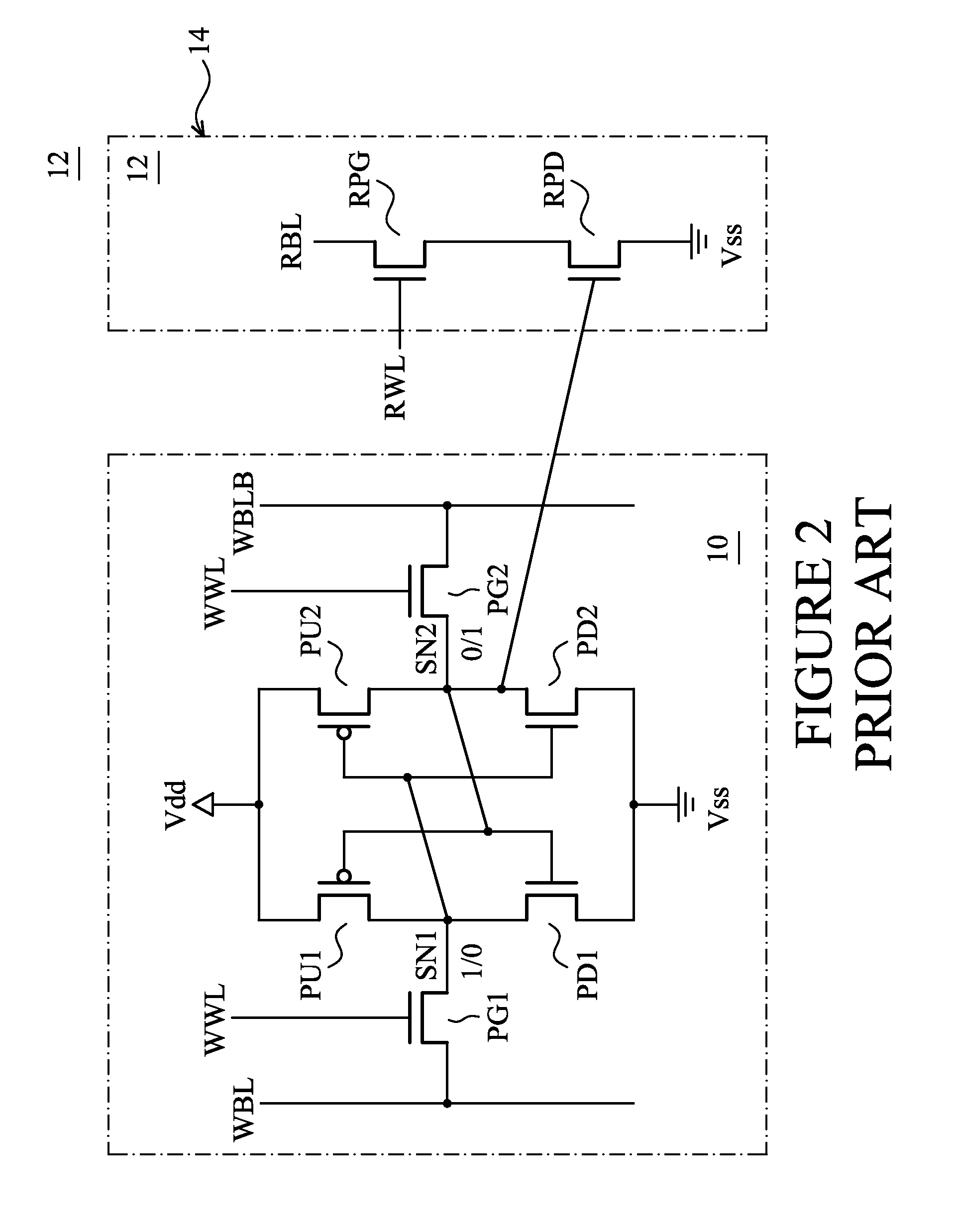
[0044]FIG. 4 depicts in one exemplary embodiment a circuit view of an 8T SRAM bit cell 40 incorporating the dual gate oxide features of the invention. In FIG. 4, the 6T storage cell portion 42 has two PMOS pull up transistors PU1 and PU2 as shown in FIGS. 1, 2 and 3; and four NMOS transistors PG1 and PG2, PD1, and PD2 also as shown in the above referenced figures. In this embodiment, however, a thicker gate dielectric is used to form the four NMOS transistors. By using a thicker gate dielectric, the standby current Isb for the SRAM storage cell portion 42 is reduced and stabi...


PUM


Abstract

Circuits and methods for providing an SRAM or CAM bit cell. In one embodiment, a bit cell portion with thicker gate oxides in the storage cell transistors, and thinner gate oxides in a read port section having transistors are disclosed. The use of the thick gate oxides in the storage cell transistors provides a stable storage of data and lower standby leakage current. The use of the thinner gate oxides in the read port transistors provides fast read accesses and allows a lower Vcc,min in the read port. The methods used to form the dual gate oxide thickness SRAM cells have process steps compatible with the existing semiconductor manufacturing processes. Embodiments using high k gate dielectrics, dual gate dielectric materials in a single bit cell, and using finFET and planar devices in a bit cell are described. Methods for forming the structures are disclosed.

Description

[0001]This application claims the benefit of U.S. Provisional Application No. 61 / 243,941, filed on Sep. 18, 2009, entitled “Methods and Apparatus for SRAM Bit Cell with Low Standby Current, Low Supply Voltage and High Speed,”, which is hereby incorporated in its entirety herein.RELATED APPLICATIONS[0002]This application relates to co-pending and co-owned U.S. Provisional Patent Application Ser. No. 61 / 243,896, entitled “Embedded SRAM Memory for Low Power Applications”, which was filed on Sep. 18, 2009, and which is hereby incorporated by reference in its entirety herein.TECHNICAL FIELD[0003]The present invention relates to an SRAM memory bit cell structure and methods for providing a bit cell with improved standby leakage current (Isb) for improved standby operation, improved Vcc,min power for lowered supply levels, and high speed read access times. The bit cell includes an innovative layout and multiple gate oxide thicknesses within cell transistors. The use of the invention provid...

Claims


Application Information

Patent Timeline
Patent Type & Authority Patents(United States)
IPC IPC(8): H01L27/12H01L21/70
CPCG11C11/412H01L27/105H01L27/11H01L27/1104H01L27/1116H01L27/0207H10B10/18H10B10/00H10B10/12
Inventor WANG, PING-WEIYANG, CHANG-TAMII, YUH-JIER
Owner TAIWAN SEMICON MFG CO LTD
Why Eureka
Try Eureka