Semiconductor photodiode device and manufacturing method thereof

a technology of semiconductors and diodes, applied in semiconductor devices, solid-state devices, radiation controlled devices, etc., can solve the problems of poor absorption, scarce light absorption, high technical barriers, etc., and achieve the effect of reducing dark current and good crystallinity

Inactive Publication Date: 2012-10-23
HITACHI LTD
View PDF11 Cites 4 Cited by
  • Summary
  • Abstract
  • Description
  • Claims
  • Application Information

AI Technical Summary

Benefits of technology

[0009]Optical communication has become predominant in broad band networks of internets that form a part of the foundation of modern information society. In the optical communication system, near infrared (IR) light within a range of 800 nm to 1600 nm is used. A particularly important wavelength band is a band where loss of optical fibers becomes minimum, and 850 nm is used for short distant communication and 1300 nm and 1550 nm are used for long distance communication. For photodiode devices in the optical communication, compound semiconductors, mainly, gallium arsenide (GaAs) and indium phosphide (InP) having good light absorbing characteristics in the long wavelength band have been used. However, for further popularization of future optical communication system, it is essential to reduce the cost and the size and, further, improve the performance of apparatus, and technical innovation is demanded also for the photodiode devices in order to attain such demands.
[0010]Means for addressing the subject described above includes integration of a photodiode device on a silicon chip. With respect to silicon (Si), refinement and high integration of transistors have been progressed under the background of matured process techniques and this is a material indispensable for integrated circuits. When a technique of hybridizing the photodiode device on Si can be established, integration circuits and optical devices can be integrated on one chip, which can solve the subject described above and enable higher function and higher value addition, and it is expected to bring about remarkable industrial innovation. As a method of hybridizing the photodiode device on Si, while it may be considered a technique of bonding a compound semiconductor on an Si substrate or a method of growing crystals of a compound semiconductor on the Si substrate. However, since a large difference of the thermal expansion coefficient and the lattice constant present between the compound semiconductor and Si, or the electric polarity of the compound semiconductor deteriorates the crystallinity of the compound semiconductor, there is a high technical barrier. If Si or Si type group IV semiconductor has a photoreceiving function, the process barrier is lowered outstandingly and optical device / electronic device can be fused easily.
[0011]However, Si has a band gap of about 1.1 eV at a room temperature and scarcely absorbs light at a wavelength of 1100 nm or more. The absorption is poor also for the light at 850 nm, and the absorption length defined by a distance where the amount of an absorbed light is decayed to 1 / e layer than is 20 μm and it is difficult to use Si as a practical device. On the contrary, germanium (Ge) also belonging to the same group IV semiconductor as Si has a band gap as small as about 0.6 eV at a room temperature and can absorb a light up to 1600 nm. FIG. 2 shows a graph plotting the absorption length to the wavelength of light on various materials. Ge has an absorption length of 2 μm or less in a wavelength region of 800 nm to 1600 nm and can form a practical photodiode device. Further, since it belongs to the same group IV semiconductor as Si, it has good matching property with an Si process. Accordingly, if a photodiode device formed of Ge can be fabricated on an Si substrate, it is possible to overcome the technical barrier in view of the characteristic / process that hinders fusion of optical device / electronic device.

Problems solved by technology

However, since a large difference of the thermal expansion coefficient and the lattice constant present between the compound semiconductor and Si, or the electric polarity of the compound semiconductor deteriorates the crystallinity of the compound semiconductor, there is a high technical barrier.
However, Si has a band gap of about 1.1 eV at a room temperature and scarcely absorbs light at a wavelength of 1100 nm or more.
The absorption is poor also for the light at 850 nm, and the absorption length defined by a distance where the amount of an absorbed light is decayed to 1 / e layer than is 20 μm and it is difficult to use Si as a practical device.
However, since the Ge has a lattice constant larger by 4% than Si, strain energy is accumulated in a Ge film formed on an Si substrate by epitaxial growing and strain is moderated at or more than film thickness which is called as a critical film thickness, thereby causing crystal defects.
In a photodiode device where crystal defects are present, a current flows even when optical signals are not present (dark current), which greatly lower the sensitivity of the photodiode device.

Method used


Image

  • Semiconductor photodiode device and manufacturing method thereof
  • Semiconductor photodiode device and manufacturing method thereof
  • Semiconductor photodiode device and manufacturing method thereof

Examples


first embodiment

[0091]In this embodiment, a low defect density Ge photodiode device formed above a silicon substrate with Ge island using a low temperature germanium buffer layer being as a nuclei, as well as a manufacturing method thereof.

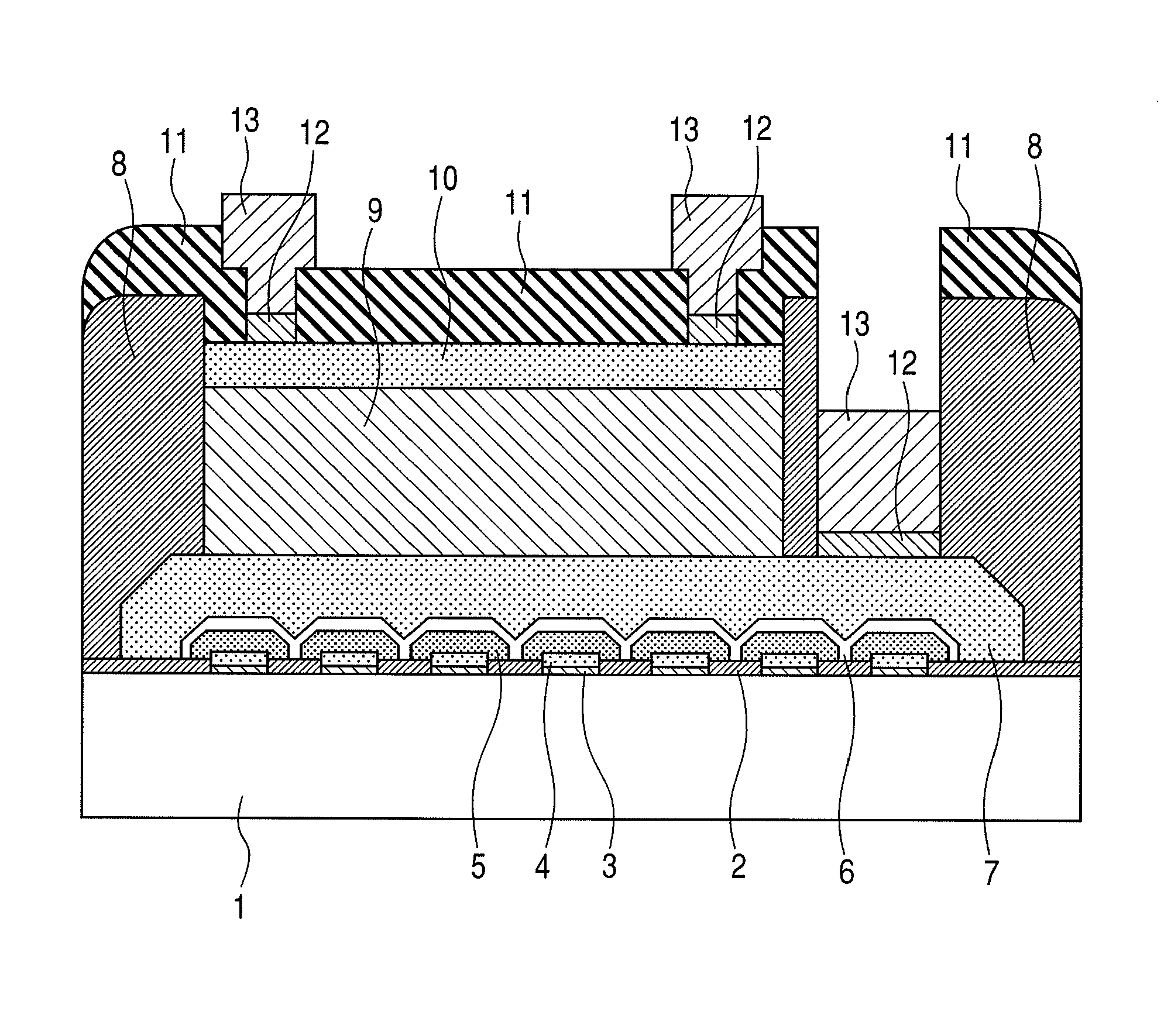
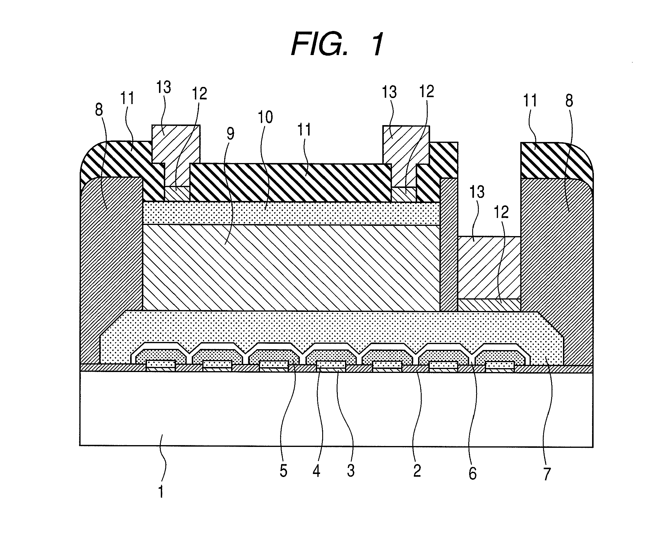
[0092]FIG. 1 is a cross sectional structural view showing a first embodiment of a semiconductor photodiode device according to the invention. This cross sectional structure shows a structure of a photodiode portion in a bipolar phototransistor having a photodiode portion and an amplification portion separately.

[0093]Reference numeral 1 in FIG. 1 denotes a silicon (Si) substrate. Above the Si substrate 1, a patterned insulating film 2, a Ge buffer layer 3 grown at a low temperature and a Ge layer 4 are formed by selective epitaxial growing in an opening window opened in the insulating film 2. On the Ge layer 4, a Ge layer 5 is grown in the perpendicular direction and the horizontal direction to the substrate by epitaxial lateral growth so as to cover the Ge layer ...

second embodiment

[0114]FIG. 14A and FIG. 14B are surface views showing a second embodiment of a semiconductor photodiode device according to the invention. FIG. 14A shows the surface after applying patterning for forming Ge islands above an Si substrate 1. FIG. 14A shows a characteristic feature that a repetitive pattern period of the Ge windows is off-set by one-half period. FIG. 14B shows a surface view in which a low temperature grown Ge layer 6 substantially buries Ge islands in the pattern shown in FIG. 14A. It can be seen that the area of the spacing remaining in the step where adjacent Ge islands coalesce to each other is decreased compared with that in the case of the first embodiment (FIG. 11B). Therefore, the thickness of the low temperature grown Ge layer 6 necessary for burying the spacing can be decreased. Since the defects incorporated in the film is decreased more as the thickness of the low temperature grown Ge layer 6 is decreased further the defect density can be decreased further ...

third embodiment

[0115]FIG. 15A and FIG. 15B are surface views showing a third embodiment of a semiconductor photodiode device according to the invention. FIG. 15A shows a surface after applying patterning for forming a Ge island above an Si substrate 1. The embodiment of FIG. 15A shows a characteristic feature that the Ge window has a rectangular shape having a length equal with the diameter of the window. According to this embodiment, the remaining spacing is eliminated at the instance adjacent Ge islands coalesce to each other (FIG. 15B). Accordingly, the thickness of the low temperature grown Ge layer 6 necessary for burying the spacing can be minimized, thereby enabling to decrease the crystal defect density in the low temperature grown Ge layer 6. However, if the diameter of the window is excessively long, the volume of the Ge buffer layer 3 and the Ge layer 4 formed in the window is increased making it difficult to sufficiently decrease the defects by the heat treatment after growing. Therefo...


PUM


Abstract

A semiconductor photodiode device includes a semiconductor substrate, a first buffer layer containing a material different from that of the semiconductor substrate in a portion thereof, a first semiconductor layer formed above the buffer layer and having a lattice constant different from that of the semiconductor substrate, a second buffer layer formed above the first semiconductor layer and containing an element identical with that of the first semiconductor layer in a portion thereof, and a second semiconductor layer formed above the buffer layer in which a portion of the first semiconductor layer is formed of a plurality of island shape portions each surrounded with an insulating film, and the second buffer layer allows adjacent islands of the first semiconductor layer to coalesce with each other and is in contact with the insulating film.

Description

CLAIM OF PRIORITY[0001]The present application claims priority from Japanese patent application JP 2009-182990 filed on Aug. 6, 2009, the content of which is hereby incorporated by reference into this application.FIELD OF THE INVENTION[0002]The present invention concerns a semiconductor photodiode device which is a photodiode device using a semiconductor containing germanium and a manufacturing method thereof and it particularly relates to a semiconductor photodiode device such as a germanium photodiode device of low defect density and a manufacturing method thereof.BACKGROUND OF THE INVENTION[0003]As a method of epitaxially growing Ge of low defect density on Si, a method of applying a low temperature buffer layer has been known (for example, refer to H-C. Luan, D. R. Lim, K. K. Lee, K. M. Chen, J. G. Sandland, K. Wada and L. C. Kimerling, Appl. Phys. Lett., 1999, vol. 75, pp. 2909-2911).[0004]Further, as another method of forming a Ge layer of low defect density on an Si substrate...

Claims


Application Information

Patent Timeline
Patent Type & Authority Patents(United States)
IPC IPC(8): H01L21/00H01L21/331H01L27/12
CPCH01L21/02381H01L21/0245H01L21/02505H01L21/02532H01L21/02576H01L21/0262H01L21/02639H01L21/02647H01L31/028H01L31/03921H01L31/103H01L31/1808Y02E10/547
Inventor MIURA, MAKOTOSAITO, SHINICHILEE, YOUNGKUNODA, KATSUYA
Owner HITACHI LTD
Why Eureka
Try Eureka