Magnetic sensor, magnetic head, and magnetic memory by using spin Hall devices

a technology of magnetic memory and magnetic sensor, which is applied in the field of magnetic sensor, magnetic head and magnetic memory by using spin hall devices, can solve problems such as difficulty in improving sensitivity, and achieve the effect of reducing thermal fluctuation and high-sensitivity signal detection

Inactive Publication Date: 2012-10-23
HITACHI LTD
View PDF14 Cites 34 Cited by
  • Summary
  • Abstract
  • Description
  • Claims
  • Application Information

AI Technical Summary

Benefits of technology

[0009]An object of the present invention is to provide a magnetic sensor that can reduce thermal fluctuation and realize high-sensitive signal detection by forming a magnetic layer of a spin Hall device in a single layer.
[0010]Another object of the present invention is to provide a magnetic head that can detect a direction of an external magnetic field as a signal using a spin Hall device.
[0011]Still another object of the present invention is to provide a magnetic memory that can record a signal by reversing a magnetization direction of a magnetic layer of a spin Hall device.
[0016]According to the above-described configuration, detection by charge accumulation is possible instead of detection by spin accumulation, or spin injection to a nonmagnetic spin Hall device by a single magnetic layer is possible by using a spin Hall device made of a highly nonmagnetic material of spin-orbital interaction resulting in the spin Hall effect. Therefore, the present invention can reduce thermal fluctuation and realize high-sensitive signal detection as compared with the conventional technology.

Problems solved by technology

In this magnetic multi-layer film structure, since plural magnetic layers are present in a signal read path using a memory and a sensor, the effect of magnetic noise resulting from thermal fluctuation of magnetization of the magnetic layer increases, thereby making it difficult to improve sensitivity.

Method used


Image

  • Magnetic sensor, magnetic head, and magnetic memory by using spin Hall devices
  • Magnetic sensor, magnetic head, and magnetic memory by using spin Hall devices
  • Magnetic sensor, magnetic head, and magnetic memory by using spin Hall devices

Examples


first embodiment

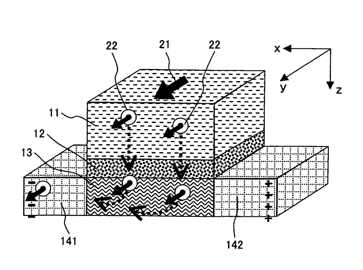
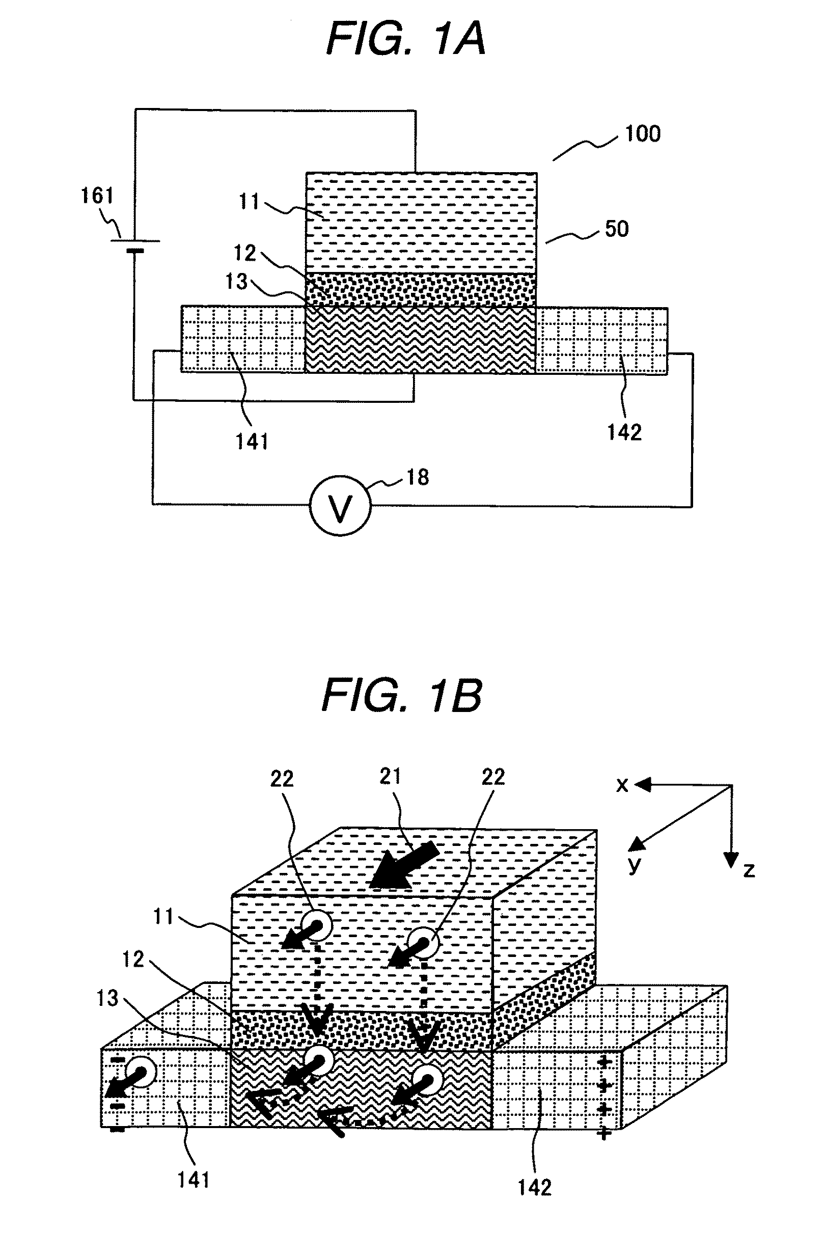
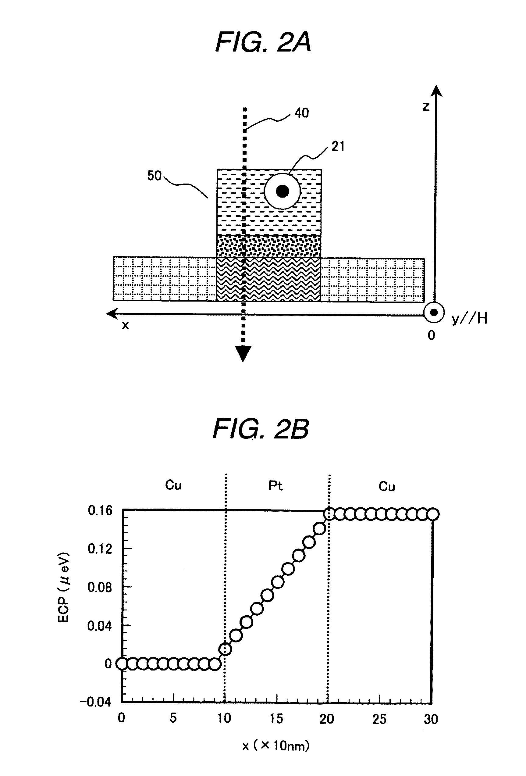
[0038]FIG. 1A shows a configuration of a magnetic sensor according to a first embodiment using the above-described spin Hall device. In a magnetic sensor 100 according to the first embodiment, a nonmagnetic body 13 that is a spin Hall layer uses an impurity-free semiconductor, a zero-gap semiconductor, or a narrow-gap semiconductor. The magnetic sensor 100 has a magnetization detection function using charge accumulation of a spin current injected from a magnetic layer 11 to the spin Hall layer 13.

[0039]As shown in FIG. 1A, a current source 161 applying a current in a film thickness direction is connected to a stacked film of a spin Hall device 50 and the current flows from the magnetic layer 11 to the nonmagnetic spin Hall layer 13. A voltage induced between two electrode terminals 141 and 142 is detected by a voltmeter 18. FIG. 1B shows the behavior of the spin current by a connection with an external circuit shown in FIG. 1A. Dotted-line arrows denote flow directions of electrons ...

second embodiment

[0044]FIG. 5A shows a configuration example of a magnetic recording head to detect a magnetic domain boundary of a perpendicular medium according to a second embodiment using the spin Hall device 51 of FIG. 4A. In a magnetic recording head (magnetic head) 200, a nonmagnetic Pt layer 13 having a width of 100 nm, a length of 100 nm, and a thickness of 40 nm is formed on a base 101 including a substrate and a base material, while a magnetic CoFe layer 11 having a width of 100 nm, a length of 100 nm, and a thickness of 40 nm is formed thereon with a nonmagnetic insulator MgO layer 12 having a width of 100 nm, a length of 100 nm, and a thickness of 60 nm between the layers 13 and 11. On a side surface of the Pt layer 13, copper (Cu) electrode terminals 141 and 142 having a width of 100 nm, a length of 100 nm, and a thickness of 40 nm are formed by a tunnel junction interposing amorphous aluminum (AlOx) 1411 and 1421. A shield 61 is formed on a side surface of a CoFe / MgO / Pt stacked film i...

third embodiment

[0051]FIG. 9A shows the basic configuration of a magnetic memory device according to a third embodiment using the spin Hall device 50 shown in FIG. 3A. A magnetic memory device 300 has a spin injection function to a magnetic layer 11 based on a charge current applied to a nonmagnetic spin Hall layer 13. In a stacked film of the spin Hall device 50 as shown in FIG. 9A, a current source 162 is connected to apply a current from an electrode terminal 141 to an electrode terminal 142 and the current flows from the electrode terminal 141 to the nonmagnetic spin Hall layer 13.

[0052]FIG. 9B shows the behavior of a spin current by a connection with an external circuit shown in FIG. 9A. Dotted-line arrows denote flow direction of electrons 22 indicated by a white ring and an arrow attached to the electron 22 denotes a spin direction. A thick arrow 21 denotes a magnetization direction of the magnetic layer 11. When a current is applied from the current source 162 to the nonmagnetic spin Hall l...


PUM

PropertyMeasurementUnit
spin diffusion lengthaaaaaaaaaa

Abstract

A magnetic sensor reduces thermal fluctuation and realizes high-sensitive signal detection using a spin Hall device of a simple structure configured with only one magnetic layer. The magnetic sensor includes a stacked film in which a nonmagnetic spin Hall layer, a nonmagnetic insulator layer, and a magnetic layer are stacked, an electrode nonmagnetic terminal pair connected to a side surface of the nonmagnetic spin Hall layer, and a unit applying a current in a film thickness direction of the stacked film. A thickness of the nonmagnetic spin Hall layer is thinner than twice a spin diffusion length of a material constituting the nonmagnetic spin Hall layer. A magnetization direction of the magnetic layer magnetized by an external magnetic field is detected due to the polarity of a voltage across both ends of the electrode nonmagnetic terminal pair.

Description

CLAIM OF PRIORITY[0001]The present application claims priority from Japanese patent application JP 2007-332150 filed on Dec. 25, 2007, the content of which is hereby incorporated by reference into this application.BACKGROUND OF THE INVENTION[0002]1. Field of the Invention[0003]The present invention relates to a magnetic sensor, a magnetic head, and a magnetic memory by using spin Hall devices.[0004]2. Description of the Related Art[0005]It has been found that electron has charge imparting electric conductivity, spin imparting magnetic property, and three degrees of internal freedom of orbital representing spatial extension of the electron and their interaction provides new properties for a material. In order to exhibit new functions by controlling the degrees of internal freedom of electrons, which are not considered in conventional electronics, instead of a semiconductor device using charge possessed by electrons, attention is being focused on the development of spintronics materia...

Claims


Application Information

Patent Timeline
Patent Type & Authority Patents(United States)
IPC IPC(8): G11B5/37G11B5/33G11B5/127
CPCG01R33/1284G11B5/374G11C11/161G11C11/18Y10T428/1107G11B5/378
Inventor SUGANO, RYOKOICHIMURA, MASAHIKOTAKAHASHI, HIROMASA
Owner HITACHI LTD
Why Eureka
Try Eureka