
Multi-part specimen holder with conductive patterns

a specimen holder and multi-part technology, applied in the direction of liquid/fluent solid measurement, instruments, machines/engines, etc., can solve the problems of inability to connect with the external power supply, difficult register-positioning of specimens, weak attachment strength, etc., to achieve easy and steady exchange of specimens, high degree of freedom of conductive structure drag, and easy and steady

Inactive Publication Date: 2012-12-18
HITACHI LTD
View PDF16 Cites 9 Cited by
  • Summary
  • Abstract
  • Description
  • Claims
  • Application Information

AI Technical Summary

Benefits of technology

The present invention provides a specimen analyzing apparatus and a specimen holder that can directly apply external voltage to a specimen without imparting mechanical force to the specimen. The apparatus and holder can mount and exchange various specimens easily and have a high degree of freedom in conductive structure design. The invention allows for the measurement of the structure, composition, and electron state of a device in an operational condition, providing valuable information on the performance of electronic elements. The technical effects of the invention include improved flexibility, ease of use, and accuracy of measurement.

Problems solved by technology

In other words, there arises a problem that a specimen incommensurate with the current conduction terminal or the shape of the conductive pattern cannot be connected with the external power supply even if the specimen can be mounted to the specimen holder or specimen stand.
Further, there arises another problem that since the difference in size is large between the specimen holder or specimen stand and the specimen, register-positioning of the specimen is difficult to perform when setting the specimen to the specimen holder or specimen stand.
But, in the technique shown in Patent Document 4, because of direct attachment to the surface of the thin-film specimen, the fine conductor or chip juts out of the fine specimen piece and structurally, the strength of attachment is weak.
To add, since the fine conductor or chip per se is bare, there is a possibility that during mount / dismount of the specimen to / from the specimen analyzing apparatus proper, the fine conductor or chip will be disconnected or cut off to be broken by vibrations applied to the thin-film specimen or conductive structures will be swung or waggled under the application of vibrations so as to be short-circuited, giving rise to a problem of troublesome exchange of the specimen.
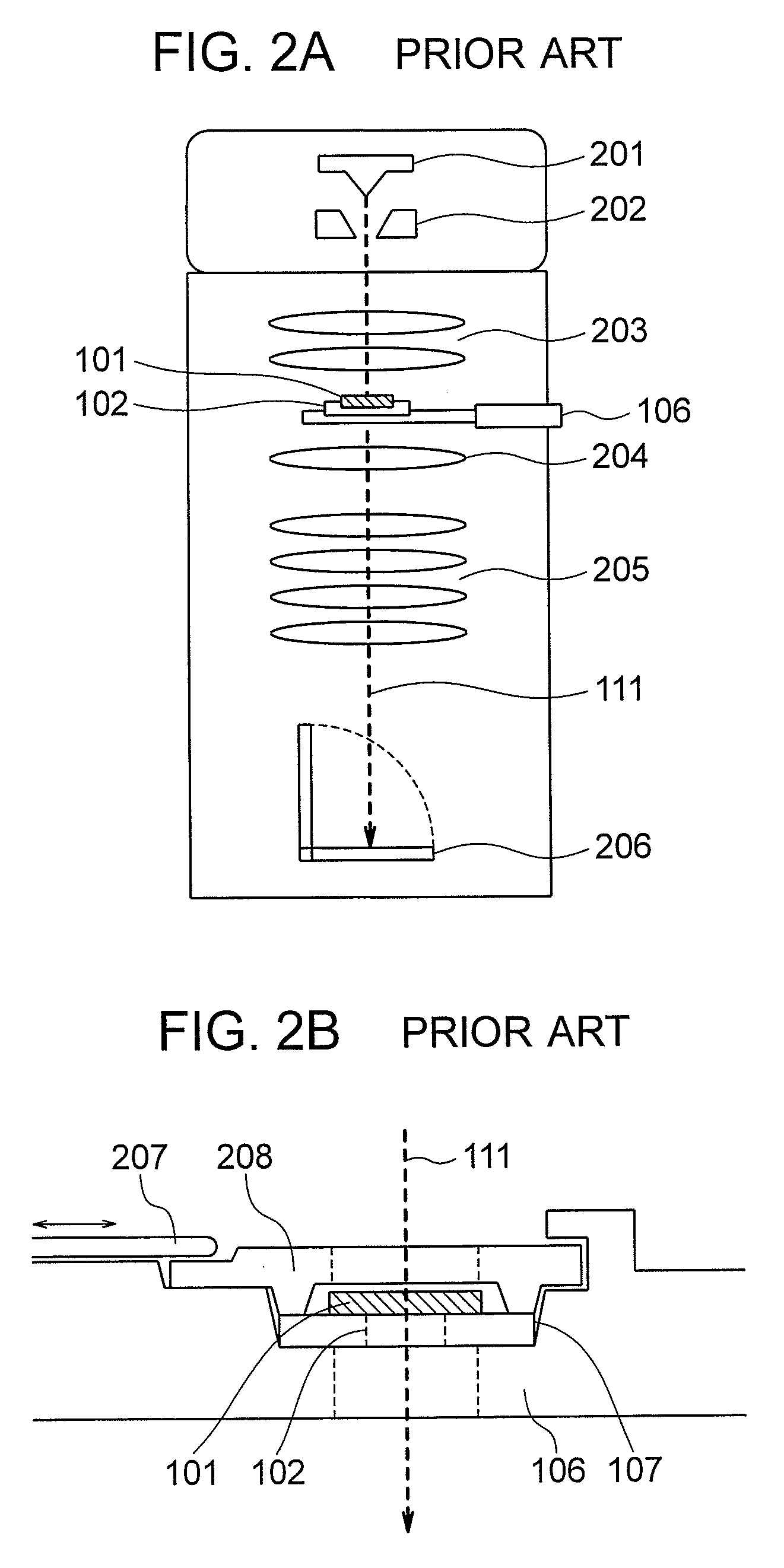
In measurement of specimens with the specimen analyzing apparatus typically represented by the transmission electron microscope, it is general practice to make, in advance of the measurement, a specimen a thin film having so small a thickness at to permit a particle beam to transmit therethrough and so, if the thin-film specimen makes direct contact with the stylus and is consequently applied with stress externally, the specimen per se is distorted because of its extreme thinness under even a weak force and there is a possibility that characteristics of a device contained in the specimen will be affected or the specimen will be broken down.

Method used


Image

  • Multi-part specimen holder with conductive patterns
  • Multi-part specimen holder with conductive patterns
  • Multi-part specimen holder with conductive patterns

Examples


embodiment 1

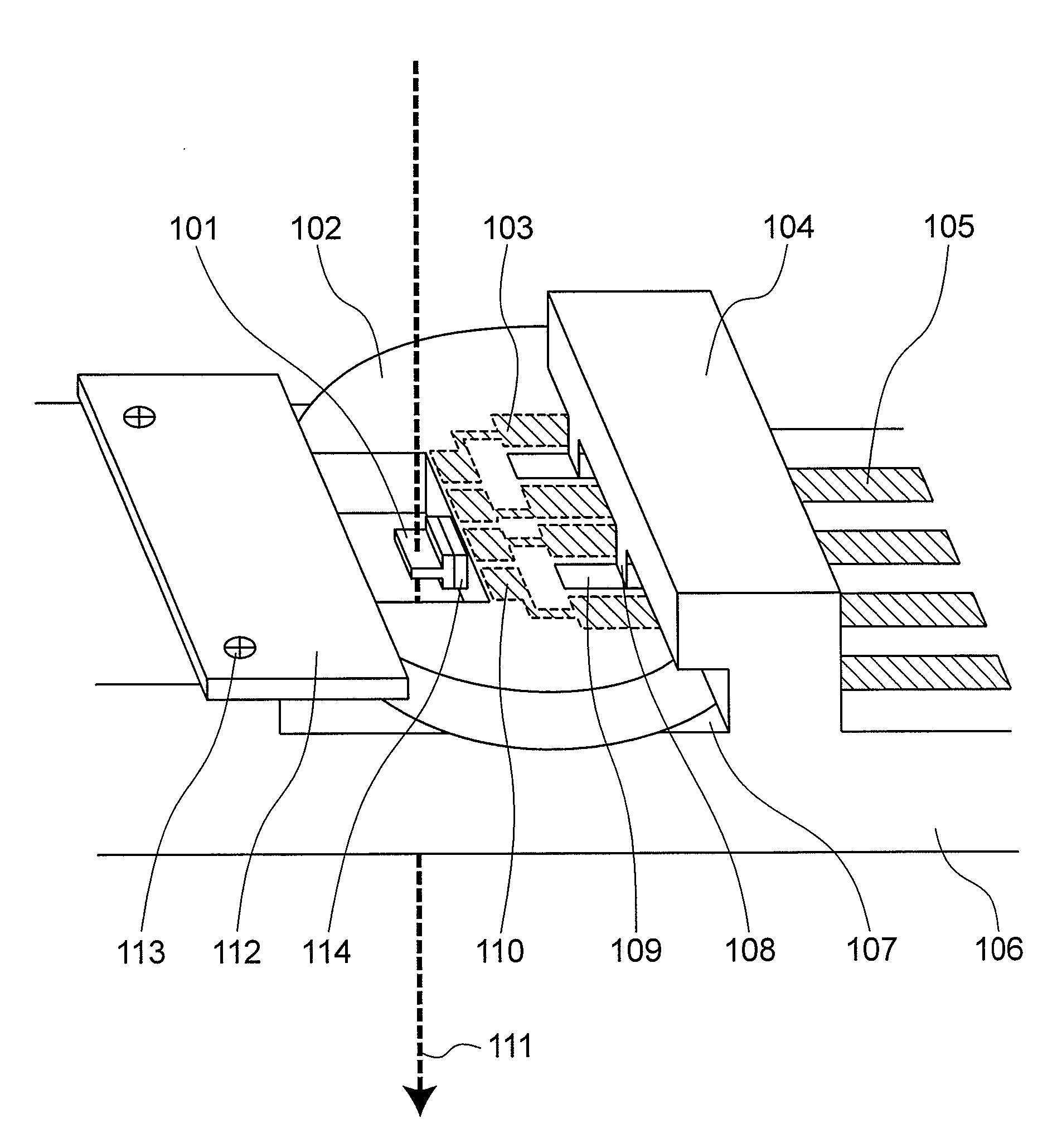
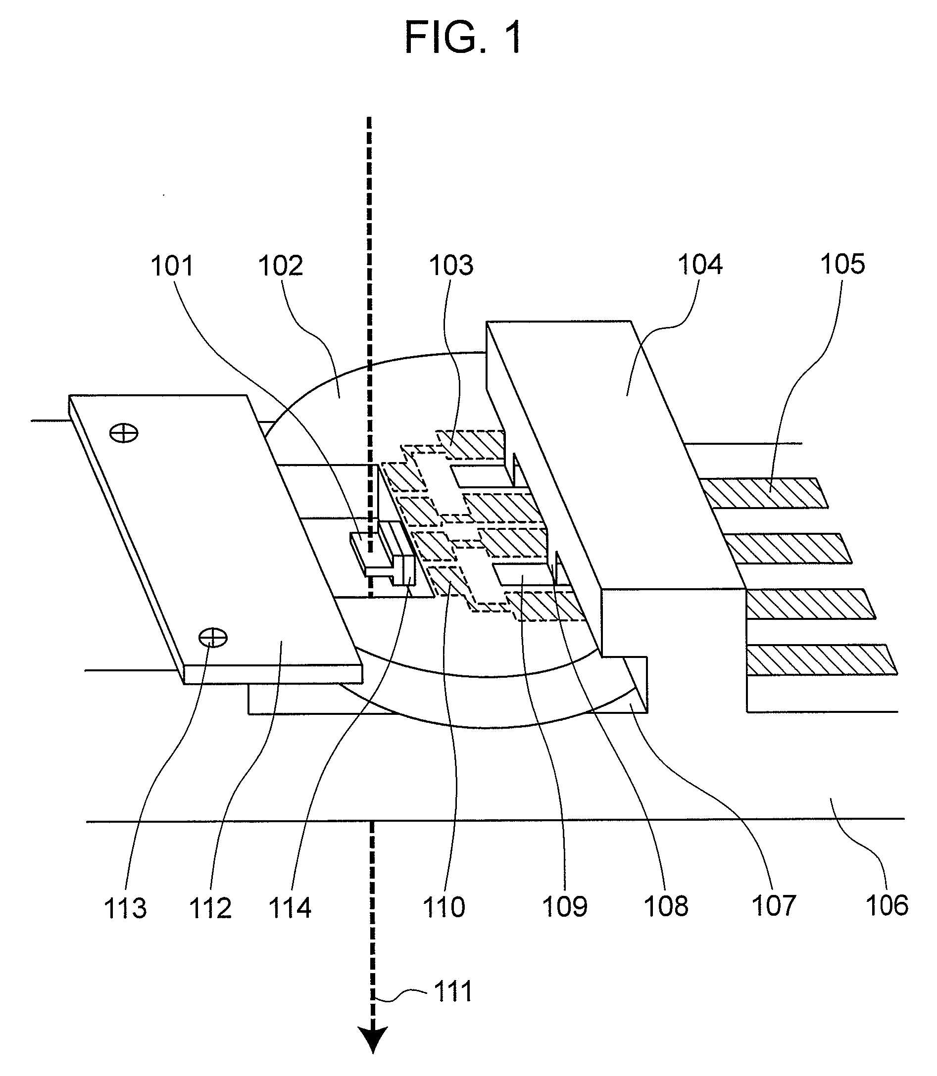
[0032]Referring first to FIG. 1, an embodiment of a specimen holder used for a specimen analyzing apparatus or the like is illustrated in perspective view form. A specimen support or mesh 102 has a single conductive structure / pattern or plural conductive structures / patterns (hereinafter referred to as a mesh electrode 103 including pad 110) connectable to an external voltage applying portion of a specimen to be observed. A mesh structure having the mesh electrode 103 will be detailed later in connection with embodiment 2.

[0033]A specimen 101 thinned precedently to a film having so a small thickness as to enable a particle beam typified by an electron beam to transmit therethrough is attached to the mesh 102 and the specimen 101 thus seated on or integral with the mesh 102 is mounted on a specimen holder 106. Alternatively, the mesh 102 may be mounted on the specimen holder 106 in advance and thereafter the thin-film specimen 101 may be attached to the mesh 102.

[0034]On the other han...

embodiment 2

[0038]In the present embodiment, the structure of the mesh in embodiment 1 will be described in greater detail.

[0039]Embodiments of the mesh 102 are illustrated in FIGS. 5A to 5G. In an embodiment shown in FIG. 5A, the mesh 102 is shaped to a form mountable and dismountable to / from the specimen holder and this form is not limited to be circular or elliptical but may be of either polygonal form or circular or elliptical form in combination with polygonal form. In another embodiment shown in FIG. 5B, the mesh 102 is provided with a handle 501 for the convenience of an operator engaged in mount / dismount of the mesh 102 to / from the specimen holder.

[0040]The mesh 102 has a mesh electrode 103 of a single conductive structure / pattern or plural conductive structures / patterns. Since the mesh electrode 103 is built in the mesh 102 in advance, a specimen to be observed can be fixedly attached on the mesh 102 to be integral therewith. Accordingly, such a structure that a fine lead conductor or ...

embodiment 3

[0045]In the present embodiment, “a method for picking out a thin-film specimen from a semiconductor wafer” and “a method for fixing a thin-film specimen to a mesh” will be described. In the former method, a specimen thinned to a film through mechanical process based on dicer or polishing may be picked out or a specimen thinned to a film through a work using a focused ion beam may be picked out. Especially, in the latter work using a focused ion beam, a “micro-sampling method” to be described later can be employed through the use of which a series of processes of picking out a thin-film specimen from a device chip or semiconductor wafer and fixing the specimen to a mesh can be executed by means of a single specimen preparation unit. The specimen preparation unit will be described with reference to FIG. 6 and a thin-film specimen preparation method based on the micro-sampling process will be detailed with reference to FIGS. 7 and 8.

[0046]Firstly, an example of the construction of the...


PUM


Abstract

In a specimen analyzing apparatus such as a transmission electron microscope for analyzing the structure, composition and electron state of an observing specimen in operation by applying external voltage to the specimen to be observed, a specimen support (mesh) including a mesh electrode connectable to external voltage applying portions of the specimen and a specimen holder including a specimen holder electrode connectable to the mesh electrode and current inlet terminals as well are provided. Voltage is applied externally of the specimen analyzing apparatus to the external voltage applying portions of the specimen through the medium of the specimen holder electrode and mesh electrode.

Description

INCORPORATION BY REFERENCE[0001]The present application claims priority from Japanese application JP2006-132084 filed on May 11, 2006, the content of which is hereby incorporated by reference into this application.BACKGROUND OF THE INVENTION[0002]The present invention generally relates to specimen analyzing apparatus represented by transmission electron microscopes and more particularly, to a specimen analyzing apparatus of the type capable of externally applying voltage or current to desired external voltage applying portions of various kinds of specimens as typified by semiconductor devices and a specimen holder for use in the specimen analyzing apparatus as well.[0003]The specimen analyzing apparatus typified by a transmission electron microscope has high spatial resolution, for which a variety of attachable analytical functions have been developed, is very efficient as a tool for fault analysis and characteristic evaluation in various electronic devices such as semiconductor dev...

Claims


Application Information

Patent Timeline
Patent Type & Authority Patents(United States)
IPC IPC(8): G01F23/00G21K5/08G21K5/10
CPCG01R31/307H01J37/04H01J37/20H01J37/28H01J37/3056H01J2237/2008H01J2237/24564H01J2237/2594H01J2237/2802H01J2237/31745H01J2237/31749
Inventor ONO, SHIANOKOGUCHI, MASANARITSUNETA, RURIKO
Owner HITACHI LTD
Learn More