Method of fabricating GaN substrate

a gallium nitride and substrate technology, applied in the direction of polycrystalline material growth, crystal growth process, after-treatment details, etc., can solve the problems of gan layer breakage, high cost and complicated process, and the method is also complicated process, and achieves low cost and high manufacturing yield. , the effect of simple process

Inactive Publication Date: 2013-01-08
SAMSUNG CORNING PRECISION MATERIALS CO LTD
View PDF37 Cites 5 Cited by
  • Summary
  • Abstract
  • Description
  • Claims
  • Application Information

AI Technical Summary

Benefits of technology

[0010]Aspects of the present invention provide a simple, low-cost method of manufacturing a freestanding gallium nitride (GaN) substrate that can achieve a high manufacturing yield.

Problems solved by technology

This method is also a complicated process that requires separate metal layer formation and etching processes (In-plane bandgap control in porous GaN through electroless wet chemical etching (Volume 80, Number 6, 11 Feb. 2002, Applied Physics Letters)).
The lift-off process may also cause breakage of the GaN layer due to thermal imbalance.
The method may provide high quality freestanding GaN but it is an expensive and complicated process that adds a risk of metal contamination.

Method used


Image

  • Method of fabricating GaN substrate
  • Method of fabricating GaN substrate
  • Method of fabricating GaN substrate

Examples


Embodiment Construction

[0024]Reference will now be made in detail to the present embodiments of the present invention, examples of which are illustrated in the accompanying drawings, wherein like reference numerals refer to the like elements throughout. The embodiments are described below in order to explain the present invention by referring to the figures.

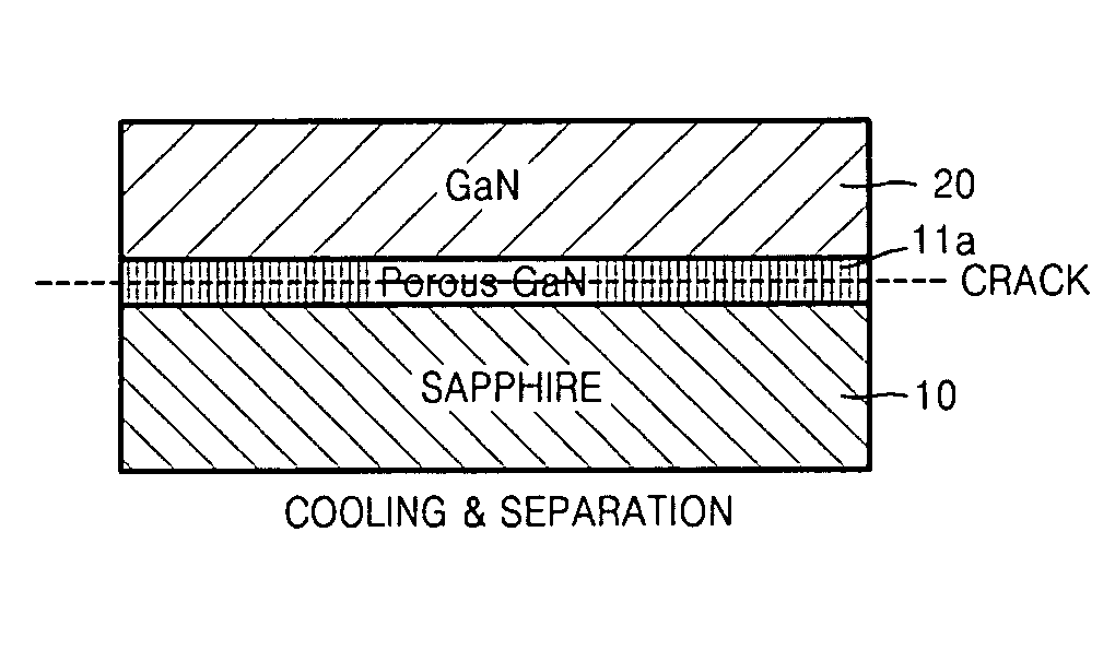
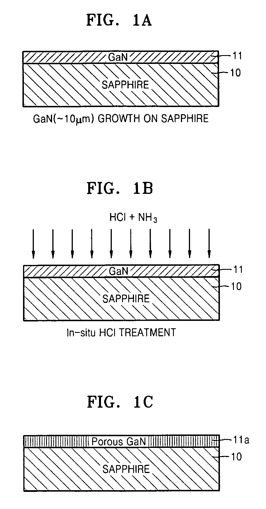
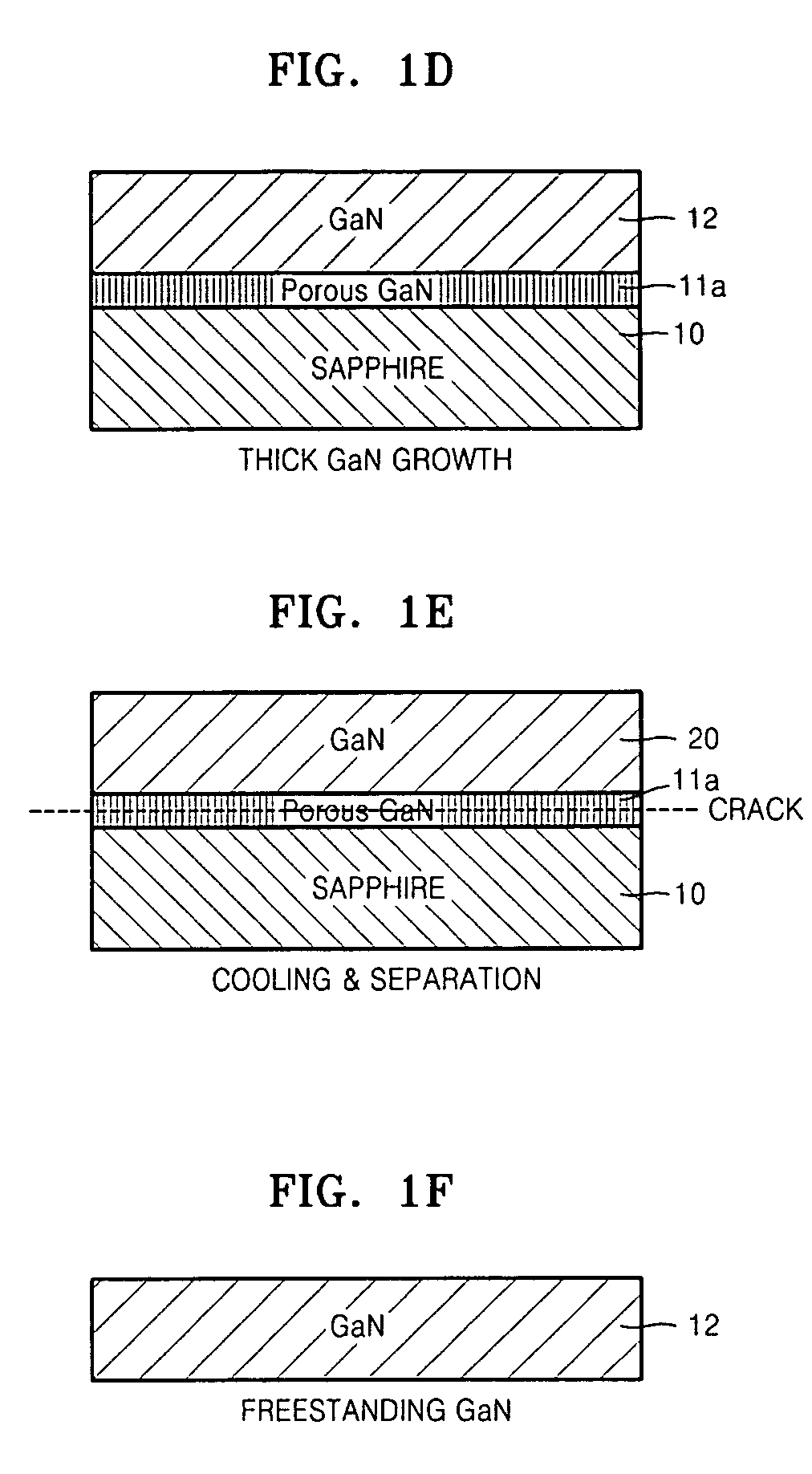
[0025]Referring to FIG. 1A, a semiconductor substrate 10, such as, for example, a sapphire substrate with a GaN layer 11 on a top surface thereof, is prepared. Although the semiconductor substrate 10 is described as a sapphire substrate, the semiconductor substrate 10 may also be any suitable material, such as, for example, a GaN or SiC substrate. For example, the substrate 10 may be a starting substrate for growth of a crystal layer. After the substrate 10 is loaded into a reactor of a hydride vapor phase epitaxy (HVPE) system, GaCl and NH3 gases are supplied as source gases along with an N2 carrier gas to form the GaN layer 11 on the substrate 10. Al...


PUM

PropertyMeasurementUnit
temperatureaaaaaaaaaa
thicknessaaaaaaaaaa
thicknessaaaaaaaaaa

Abstract

A method of fabricating a freestanding gallium nitride (GaN) substrate includes: preparing a GaN substrate within a reactor; supplying HCl and NH3 gases into the reactor to treat the surface of the GaN substrate and forming a porous GaN layer; forming a GaN crystal growth layer on the porous GaN layer; and cooling the GaN substrate on which the GaN crystal growth layer has been formed and separating the GaN crystal growth layer from the substrate. According to the fabrication method, the entire process including forming a porous GaN layer and a thick GaN layer is performed in-situ within a single reactor. The method is significantly simplified compared to a conventional fabrication method. The fabrication method enables the entire process to be performed in one chamber while allowing GaN surface treatment and growth to be performed using HVPE process gases, thus resulting in a significant reduction in manufacturing costs. The fabrication method also allows self-separation of thick GaN without cracking, thus achieving a short process time and a high manufacturing yield.

Description

CROSS-REFERENCE TO RELATED APPLICATIONS[0001]This application claims the benefit of Korean Patent Application No. 2005-96167, filed on Oct. 12, 2005, in the Korean Intellectual Property Office, the disclosure of which is incorporated herein in its entirety by reference.BACKGROUND OF THE INVENTION[0002]1. Field of the Invention[0003]Aspects of the present invention relate to a method of fabricating a gallium nitride (GaN) substrate, and more particularly, to a method of fabricating a freestanding GaN substrate that includes treating a substrate surface to form a porous GaN layer.[0004]2. Description of the Related Art[0005]Various methods have been proposed for fabricating a GaN substrate to be used as a substrate for blue and UV light-emitting devices. Most conventional GaN substrate fabrication methods include forming porous GaN on a SiC or sapphire substrate, growing thick GaN, and lifting off the thick GaN using a UV laser to obtain freestanding GaN.[0006]Mynbaeva et al. present ...

Claims


Application Information

Patent Timeline
Patent Type & Authority Patents(United States)
IPC IPC(8): C30B25/00C23C16/01C30B25/18C30B29/38H01L21/205
CPCC30B25/183C30B25/186C30B29/406C30B33/06H01L21/0237H01L21/0242H01L21/02458H01L21/02513H01L21/0254H01L21/0262H01L21/02658H01L21/02664
Inventor SONG, IN-JAEHAN, JAI-YONG
Owner SAMSUNG CORNING PRECISION MATERIALS CO LTD
Why Eureka
Try Eureka