Solid-state imaging device, method of manufacturing thereof, and electronic apparatus

a technology of solid-state imaging and manufacturing methods, which is applied in the direction of radio frequency controlled devices, instruments, television systems, etc., can solve the problems of difficult to receive a sufficient amount of light, and the image quality of the photographed image is not easily improved, so as to improve the image quality of the photographed image

Active Publication Date: 2013-01-08
SONY SEMICON SOLUTIONS CORP
View PDF8 Cites 1 Cited by
  • Summary
  • Abstract
  • Description
  • Claims
  • Application Information

AI Technical Summary

Benefits of technology

[0016]As illustrated in FIG. 21, the organic photoelectric conversion layer formed by using quinacridone has high external quantum efficiency and high sensitivity in the green wavelength range.
[0019]In addition, since the blue light is absorbed in the photoelectric conversion portion which receives the green light, the amount of the blue light incident to the photoelectric conversion portion which is disposed at the lower layer to receive the blue light is decreased. Therefore, there is a case where the white balance coefficient is increased together with the deterioration in the color balance and noise amplification occurs due to the calculation, such that the image quality may be deteriorated.
[0021]Therefore, it is desirable to provide a solid-state imaging device, a method of manufacturing thereof, and an electronic apparatus capable of improving image quality of a photographed image.
[0026]According to the invention, it is possible to provide a solid-state imaging device, a method of manufacturing thereof, and an electronic apparatus capable of improving image quality of a photographed image.

Problems solved by technology

Therefore, as the size of one pixel is further reduced, it is difficult to receive a sufficient light amount, and the image quality of the photographed image is not easily improved.

Method used


Image

  • Solid-state imaging device, method of manufacturing thereof, and electronic apparatus
  • Solid-state imaging device, method of manufacturing thereof, and electronic apparatus
  • Solid-state imaging device, method of manufacturing thereof, and electronic apparatus

Examples


first embodiment

1. First Embodiment

(A) Configuration of Device

(A-1) Configuration of Main Components of Camera

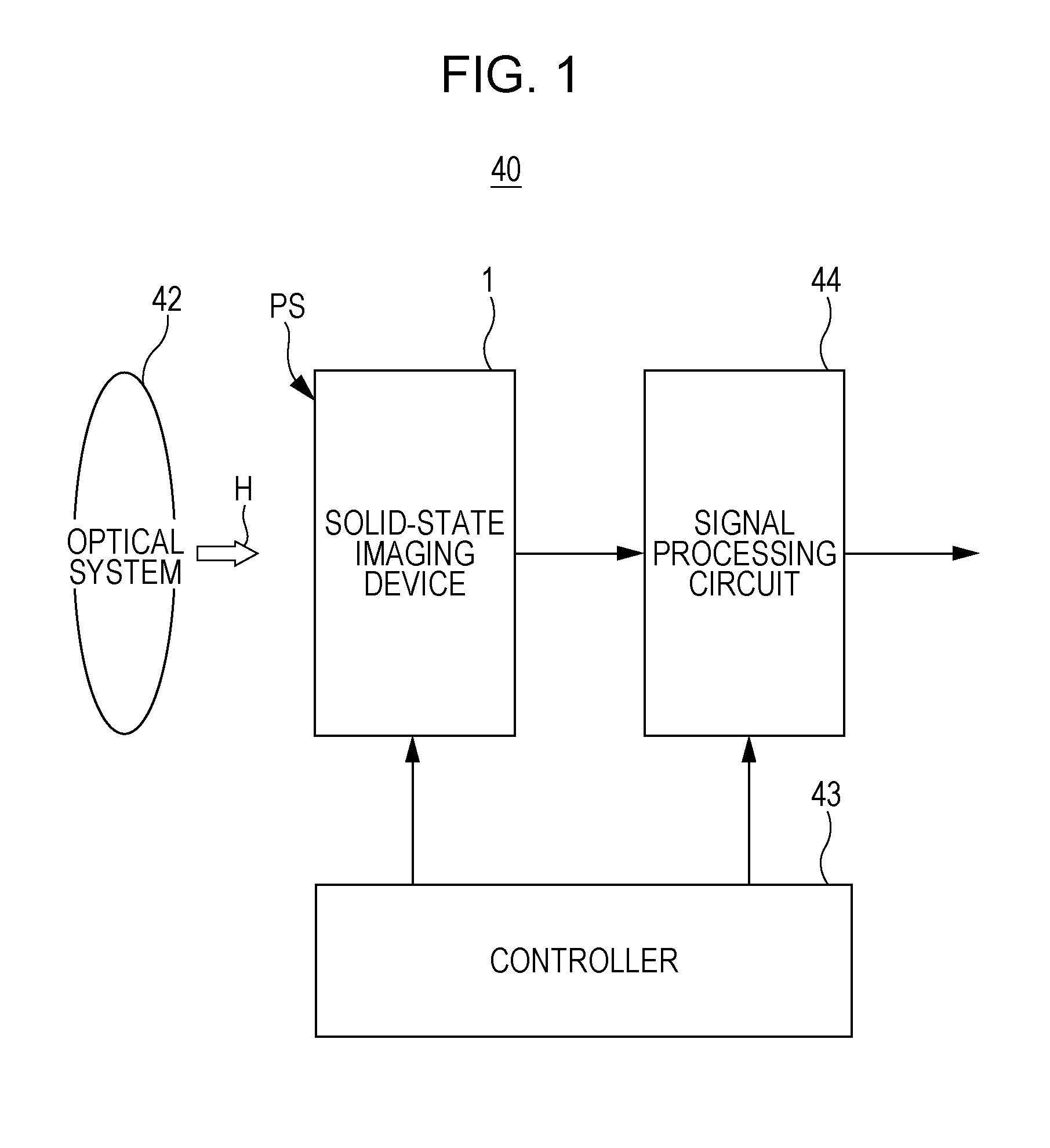
[0054]FIG. 1 is a configurational diagram illustrating a configuration of a camera 40 according to a first embodiment of the invention.

[0055]As illustrated in FIG. 1, the camera 40 includes a solid-state imaging device 1, an optical system 42, a controller 43, and a signal processing circuit 44. These components are sequentially described.

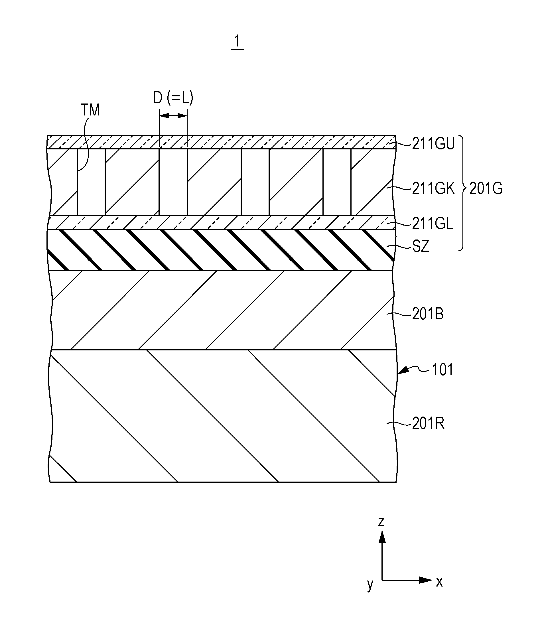
[0056]In the solid-state imaging device 1, light (subject image) H incident through the optical system 42 is sensed by an imaging area PS, and signal charges are generated by photoelectric conversion. Herein, the solid-state imaging device 1 is driven based on a control signal output from the controller 43. More specifically, the signal charges are read out and output as raw data.

[0057]The optical system 42 includes optical members such as an imaging lens or a diaphragm and is disposed so that light H incident as a subject image is focused on an imaging ar...

second embodiment

2. Second Embodiment

(A) Configuration of Device and Others

[0146]FIG. 14 is a diagram illustrating main components of a solid-state imaging device according to a second embodiment of the invention.

[0147]Herein, FIG. 14 is a diagram illustrating an organic photoelectric conversion layer 211GKb similarly to FIG. 4. Similarly to FIG. 4, FIG. 14 illustrates an upper surface of the organic photoelectric conversion layer 211GKb, and the III-III portion corresponds to FIG. 3.

[0148]As illustrated in FIG. 14, in the embodiment, the shape of the transmitting window TMb disposed in the organic photoelectric conversion layer 211GKb is different from that of the case of the first embodiment. The embodiment is the same as the first embodiment except for this point. Therefore, the description of the redundant portions is omitted.

[0149]As illustrated in FIG. 14, similarly to the first embodiment, in the organic photoelectric conversion layer 211GKb according to the embodiment, the transmitting windo...

third embodiment

3. Third Embodiment

(A) Configuration of Device and Others

[0157]FIG. 15 is a diagram illustrating main components of a solid-state imaging device according to a third embodiment of the invention.

[0158]Herein, FIG. 15 is a diagram illustrating an organic photoelectric conversion layer 211GKc similarly to FIG. 4. Similarly to FIG. 4, FIG. 15 illustrates an upper surface of the organic photoelectric conversion layer 211GKc, and the III-III portion corresponds to FIG. 3.

[0159]As illustrated in FIG. 14, in the embodiment, shapes of the organic photoelectric conversion layer 211GKc and the transmitting window TMc are different from those of the case of the first embodiment. The embodiment is the same as the first embodiment except for this point. Therefore, the description of the redundant portions is omitted.

[0160]As illustrated in FIG. 15, similarly to the first embodiment, in the organic photoelectric conversion layer 211GKc according to the embodiment, the transmitting windows TMc are ...


PUM


Abstract

Provided is a solid-state imaging device including a first photoelectric-conversion-portion selectively receiving a first wavelength light in incident light and performing photoelectric conversion; and a second photoelectric-conversion-portion selectively receiving a second wavelength light which is shorter than the first wavelength, wherein the first photoelectric-conversion-portion is laminated above the second photoelectric-conversion-portion in an imaging area of a substrate so that the second photoelectric-conversion-portion receives the light transmitting the first photoelectric-conversion-portion, wherein a transmitting portion is formed in the first photoelectric-conversion-portion so that the second wavelength light transmits the second photoelectric-conversion-portion more than other portions, and wherein the transmitting portion is formed to include a portion satisfying the following Equation within a width D defined in the direction of the imaging area, a refraction index n of a peripheral portion of the transmitting portion, and the longest wavelength λc of the second wavelength range selectively photoelectrically-converted in the second photoelectric-conversion-portion:λc / n≦2D.

Description

BACKGROUND OF THE INVENTION[0001]1. Field of the Invention[0002]The present invention relates to a solid-state imaging device, a method of manufacturing thereof, and an electronic apparatus.[0003]2. Description of the Related Art[0004]Electronic apparatuses such as a digital video camera and a digital still camera include solid-state imaging devices. For example, as the solid-state imaging device, a CMOS (Complementary Metal Oxide Semiconductor) type image sensor, a CCD (Charge Coupled Device) type image sensor, or the like is included.[0005]In the solid-state imaging device, a plurality of pixels is arrayed in a matrix shape on an imaging area of a semiconductor substrate. Each pixel is provided with a photoelectric conversion portion. For example, photodiodes are disposed as the photoelectric conversion portions.[0006]Among solid-state imaging devices, in the CMOS type image sensor, the pixel is configured to include semiconductor devices such as a pixel transistor other than the ...

Claims


Application Information

Patent Timeline
Patent Type & Authority Patents(United States)
IPC IPC(8): H01L27/00H01L31/18
CPCH01L27/146Y02E10/549Y02P70/50H10K39/32H01L27/14625H01L27/14647
Inventor TODA, ATSUSHI
Owner SONY SEMICON SOLUTIONS CORP
Why Eureka
Try Eureka