
Semiconductor device having vertical channel transistor and manufacturing method of the same
a technology of vertical channel transistor and semiconductor substrate, which is applied in the direction of semiconductor devices, basic electric elements, electrical equipment, etc., can solve the problems of body floating phenomenon, buried bit lines by etching semiconductor substrates, and difficulty in meeting the required device area, so as to reduce the resistance of bit lines and reduce the design rule
- Summary
- Abstract
- Description
- Claims
- Application Information
AI Technical Summary
Benefits of technology
Problems solved by technology
Method used
Image

Examples
Embodiment Construction
[0029]Embodiments of the present invention will be described below in detail with reference to the accompanying drawings.
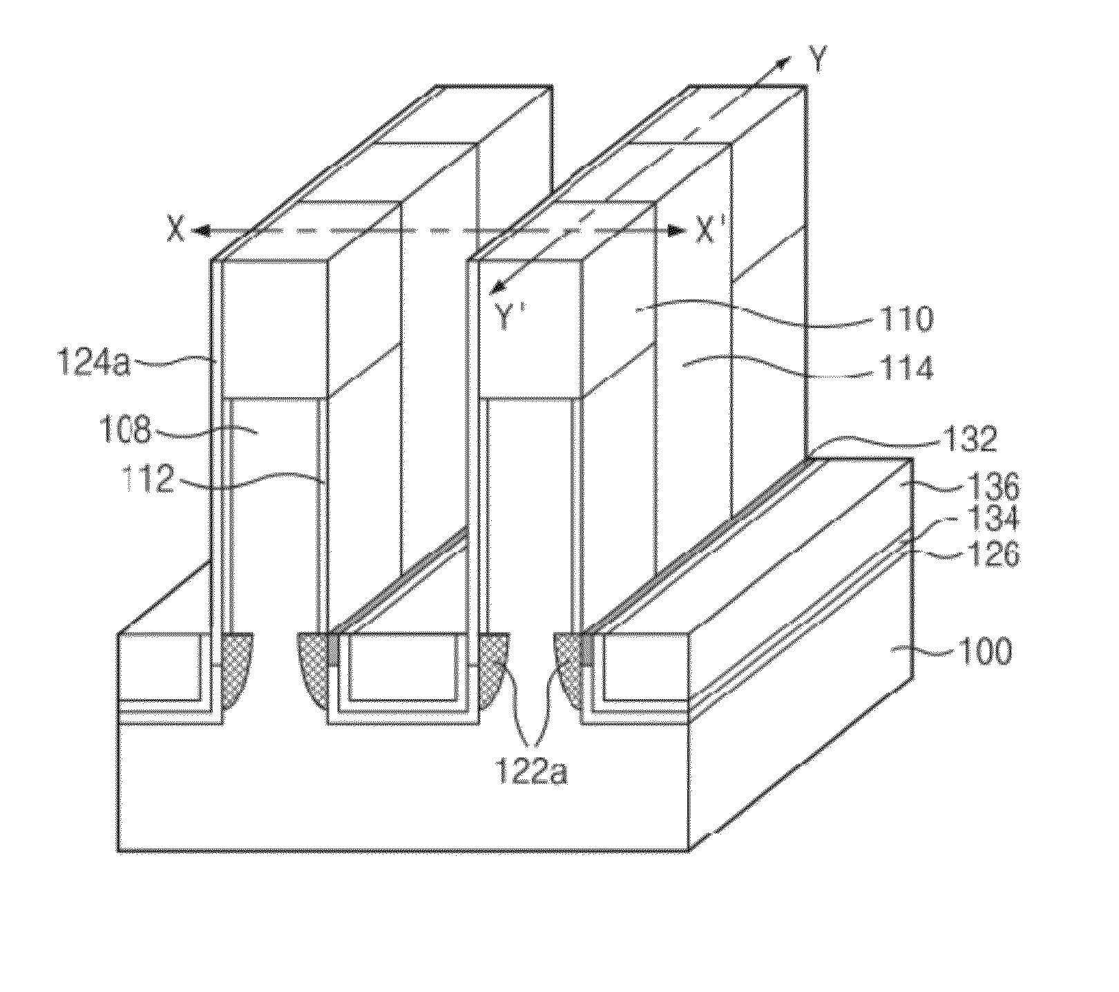
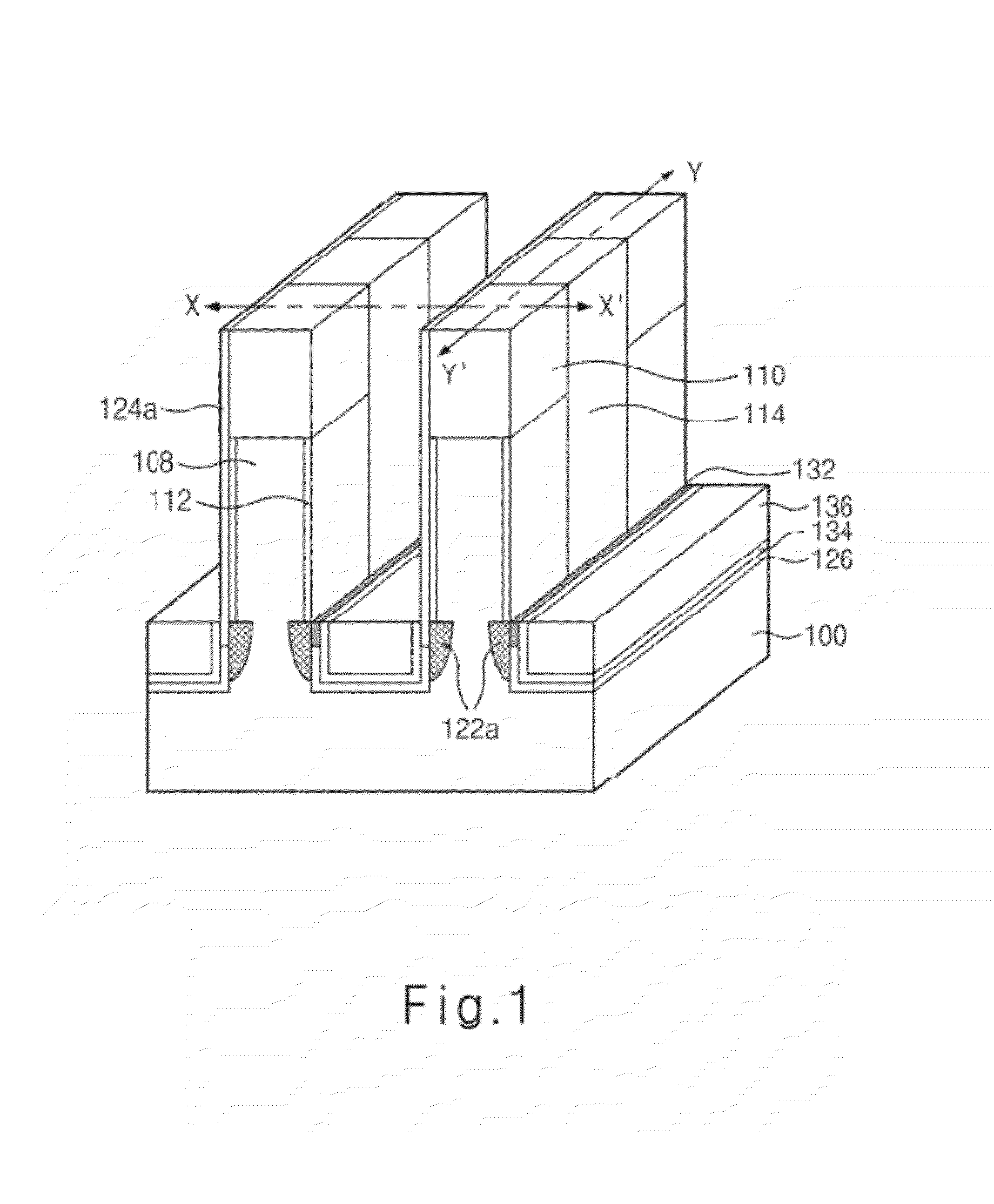
[0030]FIG. 1 is a perspective view of a semiconductor device having a vertical channel transistor according to an embodiment of the present invention.
[0031]Referring to FIG. 1, a hard mask pattern 110 is formed over a pillar 108 that is obtained by etching a silicon substrate 100. A buffer oxide film 112 is formed at a sidewall of the pillar 108. Junction regions 122a doped with impurity ions are formed in the silicon substrate 100 under the pillar 108. A titanium nitride film 134 is formed over a separation oxide film 126, and a tungsten film 136 is formed over the titanium nitride film 134. According to an embodiment of the present invention, the titanium nitride film 134 and the tungsten film 136 form a metal bit line. The bit line may be formed as high as the junction region 122a. The separation oxide film 126 separates the metal bit line from the silicon subs...
PUM
 Abstract
Description
Claims
Application Information