On-chip radiation dosimeter

a radiation dosimeter and chip technology, applied in the field of radiation monitoring and dosimetry, can solve the problems of deviating or degrading the performance of the device, affecting the accuracy of the measurement, so as to achieve the effect of higher radiation sensitivity and higher radiation sensitivity

Inactive Publication Date: 2013-01-29
GLOBALFOUNDRIES INC
View PDF19 Cites 5 Cited by
  • Summary
  • Abstract
  • Description
  • Claims
  • Application Information

AI Technical Summary

Benefits of technology

[0007]In one aspect, a method for forming a semiconductor device includes forming an implant mask on a substrate, such that a first portion of the substrate is located under the implant mask, and a second portion of the substrate is exposed; performing oxygen ion implantation of the substrate; removing the implant mask; and forming a first field effect transistor (FET) on the first portion of the substrate, and forming a second FET on the second portion of the substrate, wherein the second FET has a higher radiation sensitivity than the first FET.
[0008]In another aspect, a semiconductor device includes a first field effect transistor (FET) located on a substrate; and a second FET located on the substrate, the second FET comprising a first buried oxide (BOX) region located underneath a channel region of the second FET, wherein the first BOX region of the second FET is configured to cause the second FET to have a higher radiation sensitivity that the first FET.

Problems solved by technology

However, Geiger counters and ionization detectors are relatively expensive devices.
If a significant amount of holes are trapped in the SiO2, the threshold voltage of the device will shift, leading to deviated or degraded device performance.
As device size continues decreasing with aggressive CMOS scaling, achieving and maintaining the threshold voltage of relatively small transistors is an important and challenging task.
Creation of holes in SiO2 during the CMOS processing compromises the scaling efforts by causing device performance variations.
Additionally, in today's globalized business and marketing network, electronics products may be exposed to ionizing radiation during various activities that occur during normal business activities such as shipping (such as X-ray at airports) or even potentially from sabotage.
Such ionizing radiation exposure may be accidental, incidental, or intentional.
Throughout the entire manufacturing and supply chain, there exist numerous occasions when the chips may be damaged due to ionizing radiation exposure by sources that cause instant or progressive degradation.

Method used


Image

  • On-chip radiation dosimeter
  • On-chip radiation dosimeter
  • On-chip radiation dosimeter

Examples


Embodiment Construction

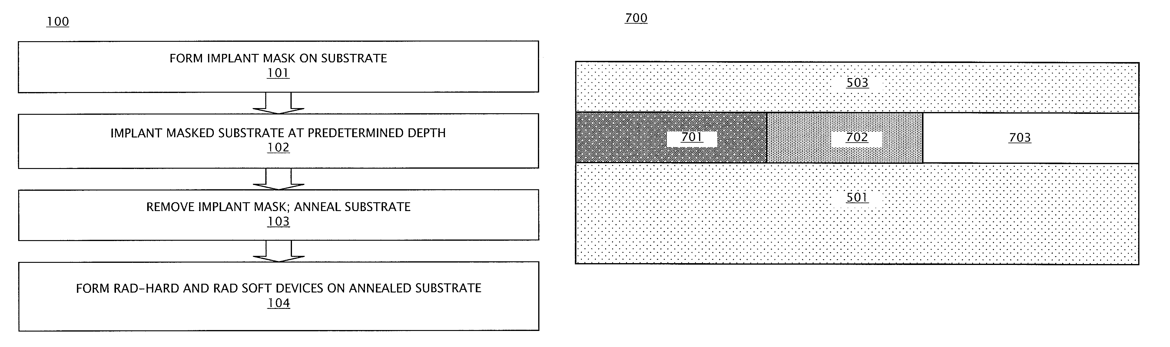
[0026]Embodiments of an on-chip radiation dosimeter, and methods of making an on-chip radiation dosimeter, are provided, with exemplary embodiments being discussed below in detail. To quantitatively track the radiation history of an electronic device such as a CMOS chip, an FDSOI on-chip radiation dosimeter may be formed on the electronic device. The FDSOI dosimeter is fabricated such that it is embedded on the device chip and experiences the same dosage of radiation during the life of the chip as the active devices. The FDSOI dosimeter may have a higher sensitivity to radiation than active devices located on the same chip, allowing for accurate measurement of the radiation exposure experienced by the chip at any stage in the life cycle of the chip by measuring the change in the threshold voltage (Vth) of the FDSOI dosimeter. This radiation exposure information may then be used to verify whether any processing steps has a potential impact on the device performance, and / or the whethe...


PUM


Abstract

A method for forming a semiconductor device includes forming an implant mask on a substrate, such that a first portion of the substrate is located under the implant mask, and a second portion of the substrate is exposed; performing oxygen ion implantation of the substrate; removing the implant mask; and forming a first field effect transistor (FET) on the first portion of the substrate, and forming a second FET on the second portion of the substrate, wherein the second FET has a higher radiation sensitivity than the first FET.

Description

BACKGROUND[0001]This disclosure relates generally to the field of radiation monitoring and dosimetry.[0002]Radiation comes in various forms, including neutrons, x-ray, γ-ray, β-ray or α-particle emission. There are many types of radiation monitors that may be used to determine an amount of radiation exposure, such as ionization detectors, Geiger counters, and thermoluminescent detectors (TLDs). Geiger counters and ionization detectors may determine and display a dose rate (for example, in mRad / hr) or an integrated dose (for example, in Rads) of radiation exposure in real time. Alarm set points may be programmed based on the dose rate or the integrated dose. A Geiger counter or ionization detector may communicate with a computer for data logging or firmware updates. However, Geiger counters and ionization detectors are relatively expensive devices. TLDs allow determination of a dose of radiation based on emission of photons in response to application of heat. TLDs may be comparativel...

Claims


Application Information

Patent Timeline
Patent Type & Authority Patents(United States)
IPC IPC(8): H01L23/552H01L31/08G01T1/24H01L27/14
CPCH01L21/26533H01L21/84H01L27/1203H01L21/76243H01L21/3115H01L31/119H01L2924/0002H01L2924/00G01T1/026H01L31/112H01L31/1804H01L21/74
Inventor GORDON, MICHAEL S.RODBELL, KENNETH P.YAU, JENG-BANG
Owner GLOBALFOUNDRIES INC
Why Eureka
Try Eureka