SOI CMOS technology-based radiation detector and preparation method thereof

A radiation detection and process technology, applied in the field of microelectronics, can solve the problems of lack of protection devices, single event effect isolation, low sensitivity response, etc., and achieve the effects of extending the detection range, reducing the threshold voltage, and high storage capacity

Active Publication Date: 2014-04-09
NO 771 INST OF NO 9 RES INST CHINA AEROSPACE SCI & TECH
View PDF3 Cites 2 Cited by
  • Summary
  • Abstract
  • Description
  • Claims
  • Application Information

AI Technical Summary

Problems solved by technology

The main problems of this type of RADFET device are as follows: 1) Due to the use of bulk silicon technology, the single event effect is not effectively isolated; 2) In order to suppress the degradation of the threshold voltage of the RADFET device after radiation, generally thicker The gate oxide thickness is too high, which causes the working voltage of the RADFET device to be too high;

Method used


Image

  • SOI CMOS technology-based radiation detector and preparation method thereof
  • SOI CMOS technology-based radiation detector and preparation method thereof

Examples


Embodiment 1

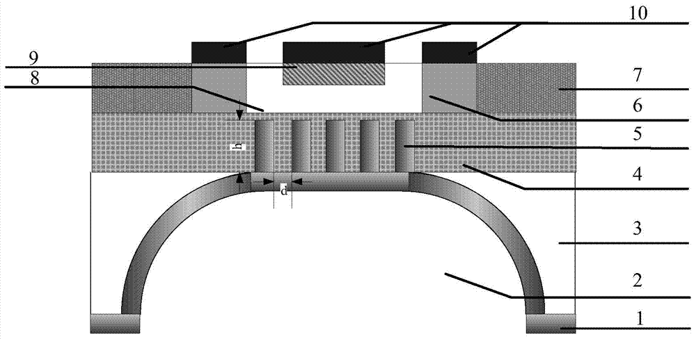
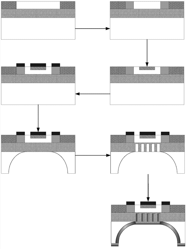
[0042] 1) On the front side of the SOI CMOS substrate, LOCOS technology is used to grow a dielectric isolation region, wherein the SOI CMOS substrate includes a Si substrate, a buried oxide layer above the Si substrate, and a Si thin film region above the buried oxide layer.

[0043] The specific steps are: removing all oxide layers on the SOI CMOS substrate, cleaning, and growing SiO with a thickness of 50nm by dry oxygen oxidation. 2 Oxygen pad layer, in which the temperature of the oxidation furnace used is 900°C, the temperature of the oxidation bottle is 85°C, and the oxidation time is 5min; then the Si with a thickness of 190nm is grown by low-pressure chemical vapor deposition (LPCVD). 3 N 4 Masking layer, wherein the deposition pressure is 25Pa, the deposition time is 30min, and the deposition temperature is 600°C; the pattern of the dielectric isolation region is photoetched by photolithography, and the dry oxidation, wet oxidation and dry oxidation are used in sequen...

Embodiment 2

[0053] 1) On the front side of the SOI CMOS substrate, LOCOS technology is used to grow a dielectric isolation region, wherein the SOI CMOS substrate includes a Si substrate, a buried oxide layer above the Si substrate, and a Si thin film region above the buried oxide layer.

[0054] The specific steps are: remove all oxide layers on the SOI CMOS substrate, clean, and grow SiO with a thickness of 125nm by dry oxygen oxidation. 2 Oxygen pad layer, in which the temperature of the oxidation furnace used is 950°C, the temperature of the oxidation bottle is 88°C, and the oxidation time is 9min; then the Si with a thickness of 210nm is grown by low-pressure chemical vapor deposition (LPCVD). 3 N 4 The masking layer, wherein the deposition pressure is 33Pa, the deposition time is 45min, and the deposition temperature is 700°C; the pattern of the dielectric isolation region is photoetched by photolithography, and the dry oxidation, wet oxidation and dry oxidation are used in sequence ...

Embodiment 3

[0064] 1) On the front side of the SOI CMOS substrate, LOCOS technology is used to grow a dielectric isolation region, wherein the SOI CMOS substrate includes a Si substrate, a buried oxide layer above the Si substrate, and a Si thin film region above the buried oxide layer.

[0065] The specific steps are: removing all oxide layers on the SOI CMOS substrate, cleaning, and growing SiO with a thickness of 100nm by dry oxygen oxidation. 2 Oxygen pad layer, in which the temperature of the oxidation furnace used is 1000°C, the temperature of the oxidation bottle is 90°C, and the oxidation time is 8min; then the Si layer with a thickness of 205nm is grown by low-pressure chemical vapor deposition (LPCVD). 3 N 4 The masking layer, wherein the deposition pressure is 27Pa, the deposition time is 55min, and the deposition temperature is 750°C; the pattern of the dielectric isolation region is photoetched by photolithography, and the dry oxidation, wet oxidation and dry oxidation are us...


PUM

PropertyMeasurementUnit
Thicknessaaaaaaaaaa
Thicknessaaaaaaaaaa
Thicknessaaaaaaaaaa

Abstract

The invention provides an SOI CMOS technology-based radiation detector and a preparation method thereof. A Si film area, a source electrode or drain electrode injection area and a medium isolation area are arranged on an oxygen-buried oxidation layer in sequence from inside to outside, a body area injection area is embedded in the Si film area, and ohmic contact electrodes are arranged on the source electrode or drain electrode injection area and the body area injection area; and a Si substrate is arranged under the oxygen-buried oxidation layer, a groove with the bottom facing upwards is arranged on the Si substrate, a back gate electrode is arranged on the surface of the groove, and a back through hole metal filling area connected with the back gate electrode is arranged inside the oxygen-buried oxidation layer. The device has high radiation sensitivity, high induced charge capacity, low working gate voltage, and high reliability. The medium isolation area grows on a front side of a substrate; the source electrode or drain electrode injection area and the body area injection area are obtained by injecting ions; the ohmic contact electrodes are obtained by sputter deposition; and a detection window area and the back through hole area are etched on the reverse side of the substrate and are filled with metal. The method is simple in technology, good in repeatability, and low in cost, and is easy to be integrated with the manufacturing technology of an existing large scale integrated circuit.

Description

technical field [0001] The invention belongs to the technical field of microelectronics and relates to semiconductor devices, in particular to a radiation detection device based on SOI CMOS technology and a preparation method thereof. Background technique [0002] Radiation detectors are mainly used to measure various radiation environmental particles, such as photons, neutrons, alpha particles, beta particles and high-energy ions. Therefore, it has a wide range of applications in nuclear physics, medical treatment, biomedical occasions, and aerospace satellite detection and other fields. For example, in the field of space applications, it is necessary to measure the metering rate of particles in the space environment in real time, so as to ensure the normal operation of electronic equipment. [0003] MOS device radiation dosimeters refer to dosimeters made of semiconductor materials. Under radiation conditions, the gate oxide dielectric region of the device will generate ...

Claims


Application Information

Patent Timeline
IPC IPC(8): H01L31/113H01L31/0352H01L31/0224H01L31/18
Inventor 杨凌
Owner NO 771 INST OF NO 9 RES INST CHINA AEROSPACE SCI & TECH
Why Eureka
Try Eureka