Laser irradiation apparatus and laser irradiation method

a laser irradiation and laser technology, applied in the field of laser irradiation apparatus and laser irradiation method, can solve the problem of restricted layout, achieve high repetition rate, increase peak power per pulse, and increase repetition rate

Active Publication Date: 2013-03-12
SEMICON ENERGY LAB CO LTD
View PDF108 Cites 36 Cited by
  • Summary
  • Abstract
  • Description
  • Claims
  • Application Information

AI Technical Summary

Benefits of technology

[0014]In order to avoid this, such a method is given that intensity distribution of a laser beam is changed into a top-flat shape, not a Gaussian shape. By having a top-flat shape, it is possible to sharpen an end portion of intensity distribution of a laser beam, thereby decreasing a crystallinity-inferior region formed after laser annealing.
[0025]In an annealing process of a semiconductor film, not only a CW laser but also a pulsed laser with high repetition rate can be used. The pulsed laser with high repetition rate has the following advantages. A period after a semiconductor film is irradiated with a laser beam and before the semiconductor film is completely solidified is said to range from several tens to several hundred ns. Therefore, if a pulsed laser with low repetition rate is used, a pulsed laser beam is delivered after a semiconductor film melted by the previous laser beam is solidified. Accordingly, at the recrytallization after the irradiation of the respective pulsed laser beams, a crystal grain grows in a radiant manner centrosymmetrically. Then, a grain boundary is formed at a boundary between the adjacent crystal grains, which causes unevenness on the surface of the semiconductor film.
[0026]When a pulsed laser with high repetition rate is used, a semiconductor film is irradiated with a laser beam after the semiconductor film is melted by the previous laser beam and before the melted semiconductor film is solidified. Therefore, unlike in the case of using a pulsed laser having low repetition rate, an interface between a solid phase and a liquid phase can be moved continuously in the semiconductor film; therefore, the semiconductor film having the crystal grain grown continuously in a direction where the laser beam is moved can be obtained.
[0027]Moreover, another advantage of the pulsed laser is that the peak power per pulse can be raised by increasing the repetition rate. Thus, it is possible to increase the conversion efficiency of a laser beam into a second harmonic even though the laser beam has a relatively low power on average. Therefore, since the higher harmonic of high power can be easily obtained, the productivity can be raised drastically.

Problems solved by technology

In such a case, it is apparent that the layout is restricted.

Method used


Image

  • Laser irradiation apparatus and laser irradiation method
  • Laser irradiation apparatus and laser irradiation method
  • Laser irradiation apparatus and laser irradiation method

Examples


embodiment modes

[0061]Embodiment modes and embodiments of the present invention will be hereinafter described with reference to the drawings. However, since the present invention can be carried out with many different modes, it is easily understood by those skilled in the art that the modes and detail of the present invention can be variously modified without departing from the scope and spirit of the present invention. Therefore, the present invention is no construed as being limited by the description of the embodiment modes and embodiments.

embodiment mode 1

[0062]An embodiment mode of the present invention is described with reference to FIGS. 1 to 4C.

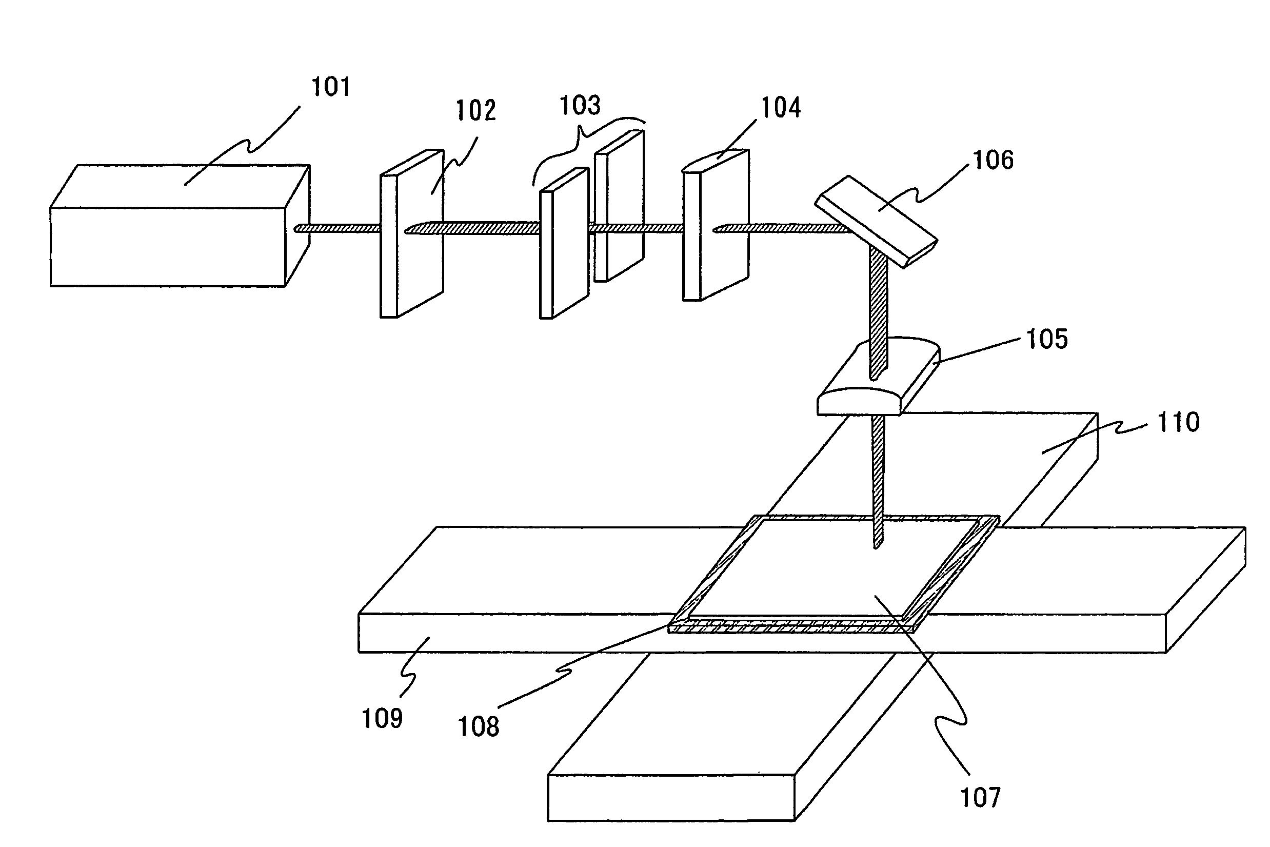
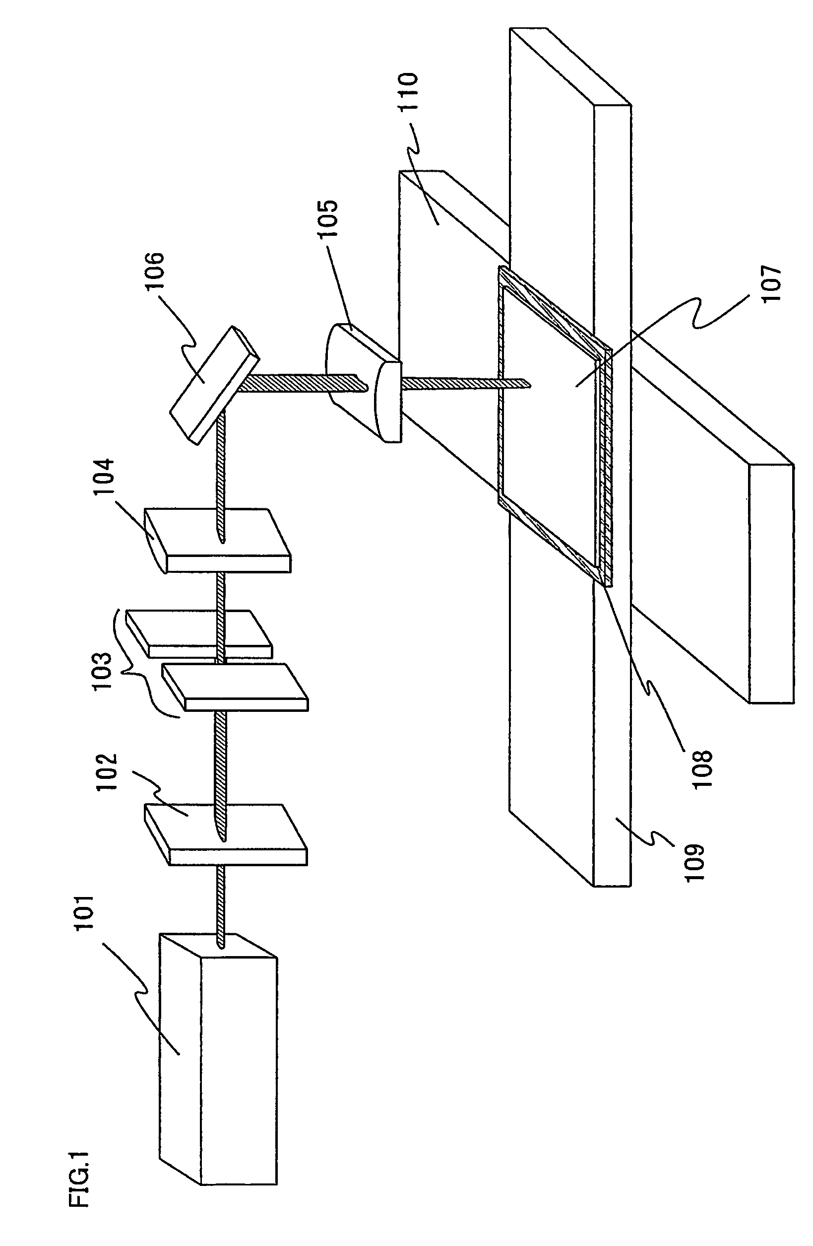
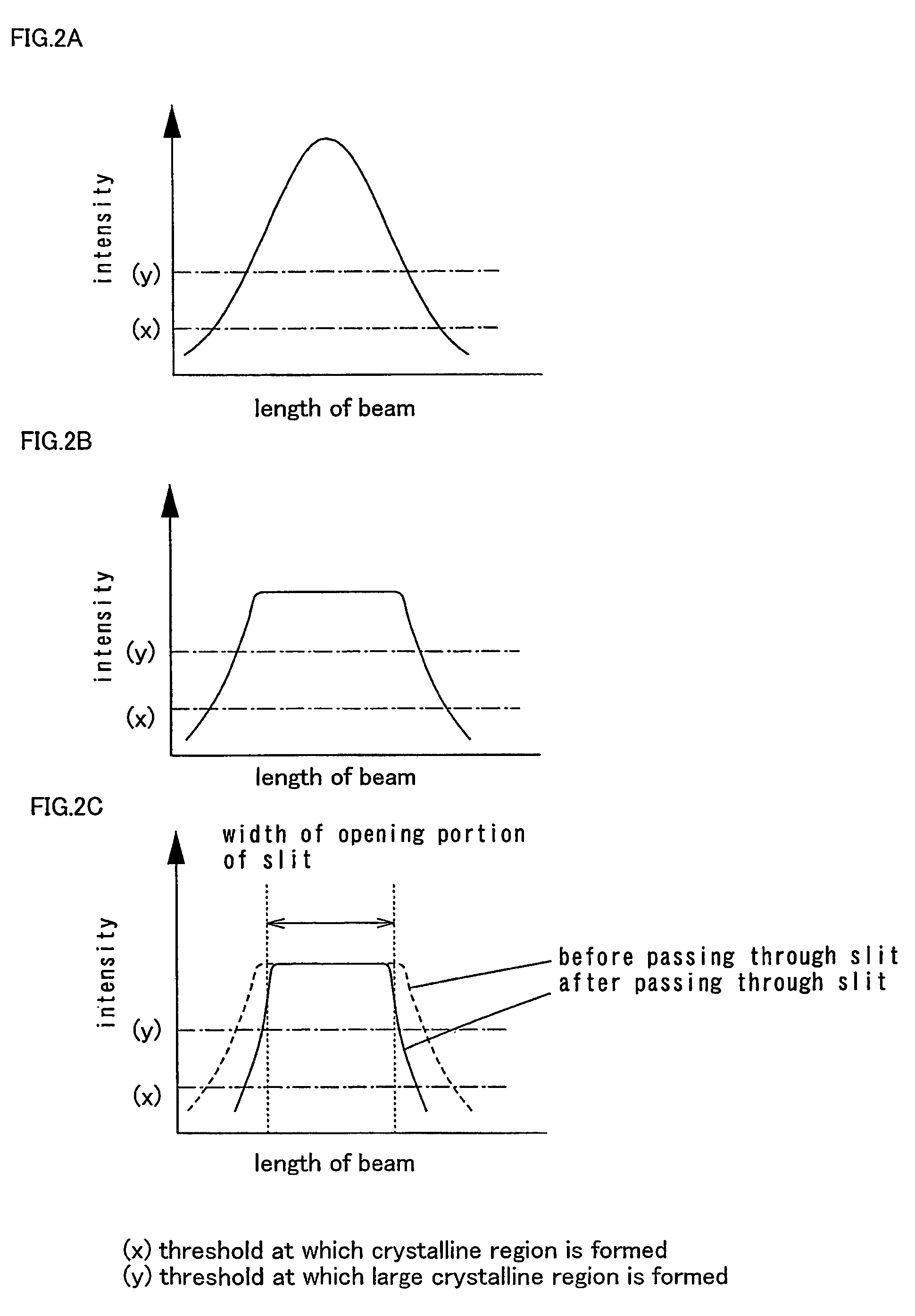
[0063]FIG. 1 shows an example of a laser irradiation apparatus. The laser irradiation apparatus includes a laser oscillator 101, a diffractive optical element (also referred to as a diffractive optics element or diffractive optics) 102, a slit 103, a projecting lens 104, and a condensing lens 105. Although the projecting lens 104 is a convex cylindrical lens in this embodiment mode, a convex spherical lens can also be used. Moreover, although the condensing lens 105 is a convex cylindrical lens, a convex spherical lens may also be used. A mirror 106 may be provided in accordance with a setting condition of an optical system in the laser irradiation apparatus.

[0064]The laser oscillator 101 may be a CW laser or a pulsed laser with a repetition rate of 10 MHz or higher. As a kind of the laser, a laser having a medium of a single-crystal YAG, YVO4, forsterite, YAlO3, or GdVO4 or a polycrystall...

embodiment mode 2

[0076]This embodiment mode will describe another optical system which is applicable in a laser irradiation apparatus of the present invention.

[0077]FIG. 5A shows an optical system used in this embodiment mode. FIG. 5B is a top view and FIG. 5C is a side view.

[0078]In Embodiment Mode 1, as shown in FIG. 5A, a convex cylindrical lens is used as the projecting lens 104 and a convex cylindrical lens is used as the condensing lens 105. Meanwhile, in this embodiment mode, a convex spherical lens is used as the projecting lens, a convex cylindrical lens is used as the condensing lens, and a concave cylindrical lens is used as a correcting lens. Except the projecting lens, the condensing lens, and the correcting lens, the same lenses as those in Embodiment Mode 1 may be used.

[0079]As shown in FIG. 5A, a laser beam emitted from a laser oscillator 501 passes through a diffractive optical element 502, whereby beam shaping and homogenization of beam intensity are carried out. Moreover, after bl...


PUM

PropertyMeasurementUnit
aspect ratioaaaaaaaaaa
thicknessaaaaaaaaaa

Abstract

A laser beam having homogeneous intensity distribution is delivered without causing interference stripes of a laser to appear on an irradiation surface. A laser beam emitted from a laser oscillator passes through a diffractive optical element so that the intensity distribution thereof is homogenized. The beam emitted from the diffractive optical element then passes through a slit so that low-intensity end portions in a major-axis direction of the beam are blocked. Subsequently, the beam passes through a projecting lens and a condensing lens, so that an image of the slit is projected onto the irradiation surface. The projecting lens is provided so that the slit and the irradiation surface are conjugated. Thus, the irradiation surface can be irradiated with the laser having homogeneous intensity while preventing the diffraction by the slit.

Description

TECHNICAL FIELD[0001]The present invention relates to a laser irradiation apparatus (apparatus including a laser and an optical system for guiding a laser beam emitted from the laser to an irradiation object) and a laser irradiation method, which are for annealing a semiconductor material or the like homogeneously and effectively. Moreover, the present invention relates to a semiconductor device manufactured by including a step of carrying out a process using these laser process apparatus and laser process method, and also relates to a manufacturing method thereof.BACKGROUND ART[0002]In recent years, a technique for manufacturing a thin film transistor (hereinafter referred to as a TFT) over a substrate has drastically progressed and development for applying a TFT to an active matrix display device has been advanced. In particular, since a TFT using a polycrystalline semiconductor film has higher electric field effect mobility (also referred to as mobility, simply) than a convention...

Claims


Application Information

Patent Timeline
Patent Type & Authority Patents(United States)
IPC IPC(8): B23K26/06B23K26/00
CPCB23K26/0738H01L27/1285H01L21/268H01L27/1266H01L21/0237H01L21/0268H01L27/1214
Inventor TANAKA, KOICHIRO
Owner SEMICON ENERGY LAB CO LTD
Why Eureka
Try Eureka