Production method of thin film transistor using amorphous oxide semiconductor film

a production method and semiconductor film technology, applied in the direction of semiconductor devices, electrical appliances, basic electric elements, etc., can solve the problems of affecting tft, dc stress affecting tft, and hardly attaining transistor characteristics, etc., to achieve effective control of resistivity, reduce dc stress, and reduce the effect of film quality degradation

Active Publication Date: 2013-04-09
CANON KK
View PDF62 Cites 136 Cited by
  • Summary
  • Abstract
  • Description
  • Claims
  • Application Information

AI Technical Summary

Benefits of technology

[0054]The introduced oxygen partial pressure as referred to herein means the partial pressure of the oxygen intentionally introduced into the interior of a film formation apparatus through a flow rate controller, not including the oxygen due to contamination such as the oxygen inevitably emitted from the internal wall and the like of the film formation apparatus, the oxygen entering from the outside because of the leakage of the film formation apparatus, and the oxygen emitted from the target. Needless to say, under such conditions that the residual oxygen gas pressure exceeds the upper limit of the above-mentioned introduced oxygen partial pressure, the advantageous effects of the present invention can hardly be attained, and hence the back pressure of the film formation apparatus to be used in the present invention is desirably 1×10⁻³ Pa or less. It is to be noted that as the above-mentioned flow rate controller, for example, a mass flow controller can be used.
[0055]In this connection, from the viewpoints of the performances and stability of the TFT device, it is desirable to form the film under the conditions that the resistivity (the first resistivity) of the metal oxide film is made to be 1 Ωcm or less, or the activation energy (the first activation energy) in the vicinity of room temperature is made to be 50 meV or less. It is to be noted that the lower limit of the resistivity of the metal oxide film on completion of the film formation is set, for example, at 1×10⁻⁴ Ωcm or more, and the lower limit of the activation energy is set, for example, at 0 meV, although these lower limits depend on the composition and the film formation conditions of the oxide film. Accordingly, the first resistivity of the present invention is desirably 1×10⁻⁴ Ωcm or more and 1 Ωcm or less, and the first activation energy of the present invention is desirably 0 meV or more and 50 meV or less.
[0056]Thereafter, the metal oxide film thus fabricated is subjected to an annealing in an oxidative atmosphere (the second step) to form the channel layer. In this case, the annealing conditions are set so that the metal oxide film has such resistivity that enables the metal oxide film to exhibit satisfactory characteristics as the TFT channel layer. For the purpose of effectively controlling the resistivity, it is recommended that the annealing is conducted by setting the temperature range in the atmosphere including oxygen as the constituent element thereof in the form of the atmosphere of oxygen, ozone, water vapor or nitrogen oxides to fall within a temperature range of 250° C. or higher and 450° C. or lower, and desirably 250° C. or higher and 350° C. or lower. Additionally, it is effective to use ozone irradiation and oxygen radical irradiation, wherein the annealing temperature can be made as low as down to 150° C. In this case, it is also a desirable mode to conduct the irradiation of ultraviolet light in ozone.
[0057]When the channel layer is formed according to the above-mentioned method, it is not necessary to precisely control the oxygen partial pressure in the film formation atmosphere because the electrical resistivity is determined by the annealing conducted after the formation of the metal oxide semiconductor film. Additionally, the metal oxide film is formed under the conditions that the metal oxide film has a low resistivity, namely, in a film formation atmosphere in which oxygen radicals and high energy oxygen negative ions are small in amount. Consequently, the electrical characteristics of the fabricated film are not varied largely as a function of the distance from the target and hence the process margin can be widened. In particular, when a metal oxide film is formed by a sputtering method, the above-mentioned effects are made remarkable; this is conceivably because the dissociation degrees of molecular gases in the vapor phase are higher as compared to other vapor phase methods.
[0058]Next, hereinafter, a production method of forming the oxide insulator protection layer (the third step) of the present invention is described.
[0059]The third step is described with reference to the inversely staggered (bottom gate) TFT illustrated in FIG. 7. It is to be noted that as for a TFT structure, a staggered (top gate) TFT may also be used.

Problems solved by technology

Additionally, there has been a problem such that the value of the optimal oxygen partial pressure is varied depending on the film formation conditions.
Additionally, a TFT adopting as the channel layer thereof an In—Ga—Zn—O film fabricated in the film formation atmosphere with oxygen introduced thereinto can hardly attain such transistor characteristics as anticipated from the physical characteristics intrinsically possessed by the In—Ga—Zn—O film.
Further, when a DC stress of a voltage of 12 V is applied for 400 seconds to each of the gate electrode and the source and drain electrodes, the characteristic variations such as the turn-on characteristic degradation and threshold voltage variation are caused, and thus the DC stress affects the TFT.
Specifically, when the film formation is conducted by using a sputtering method, conceivably the oxygen introduced into the atmosphere increases the amount of the oxygen negative ions generated on the target surface, and consequently, the amount of the high energy oxygen negative ions incident onto the substrate is increased to cause the film quality degradation.
Thus, there has been caused a problem that an atmospheric variation induces variation in electrical conductivity to destabilize the TFT operation and consequently no reliability as a device can be attained.
Additionally, the present inventors have found a problem that in the formation of an oxide insulator by sputtering on an In—Ga—Zn—O amorphous oxide thin film, the film formation in an atmosphere without oxygen contained therein causes a large variation of the electrical characteristics of the oxide semiconductor so as to prohibit the attainment of satisfactory TFT characteristics.

Method used


Image

  • Production method of thin film transistor using amorphous oxide semiconductor film
  • Production method of thin film transistor using amorphous oxide semiconductor film
  • Production method of thin film transistor using amorphous oxide semiconductor film

Examples


example 1

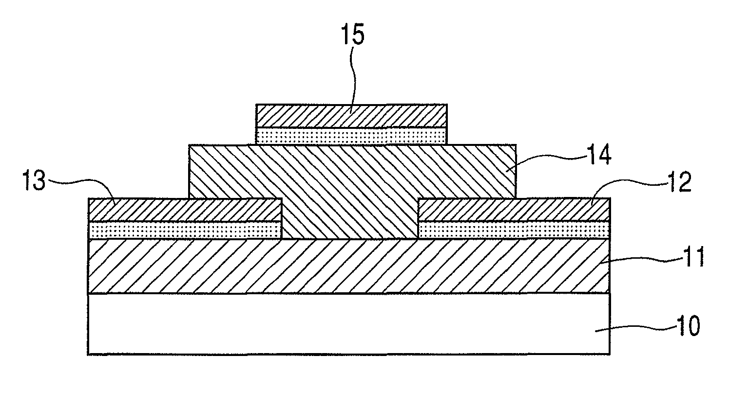
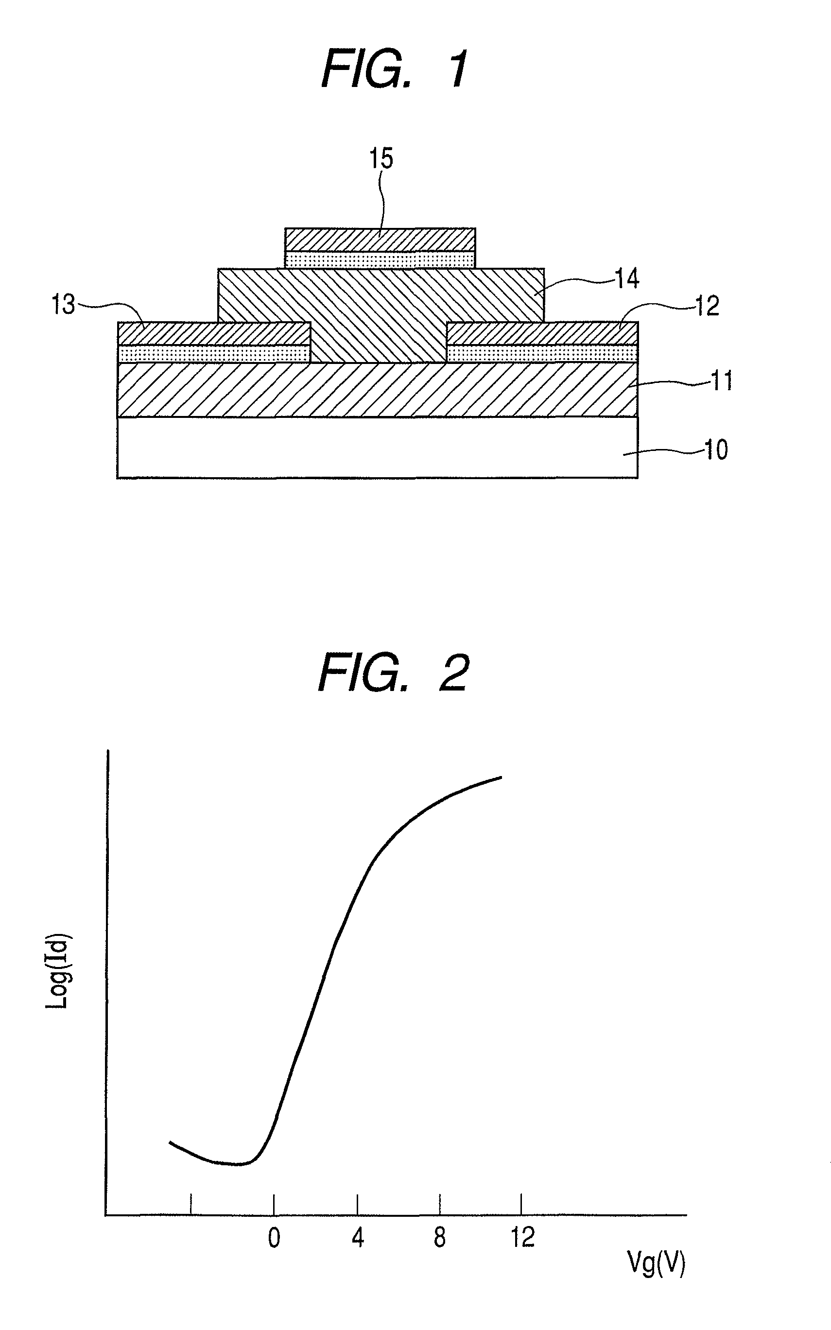
[0082]An embodiment of the TFT device of the present invention is described with reference to FIG. 1.

[0083]First, an In—Ga—Zn—O film was formed on a glass substrate 10 as a channel layer 11.

[0084]In present Example, the In—Ga—Zn—O film was formed by sputtering in an argon atmosphere and by annealing in the air.

[0085]As a target (a material source), a 2-inch sized sintered body having a composition of InGaZnO4 was used, and the applied RF power was 100 W. The distance between the target and the substrate was approximately 9 cm. The In—Ga—Zn—O film was formed in an argon atmosphere of 3.5×10⁻¹ Pa with the introduced oxygen partial pressure of 0 Pa. The substrate temperature at the time of film formation was 25° C.

[0086]Next, the In—Ga—Zn—O film fabricated by a sputtering method was annealed in the ambient air atmosphere set at 300° C. for 1 hour. The obtained film was subjected to a four-probe measurement, and the following results were obtained: the In—Ga—Zn—O film before the anneali...

example 2

[0092]An embodiment of the TFT device in the present invention is described with reference to FIG. 1.

[0093]First, an In—Ga—Zn—O film was formed as a channel layer 11 on a glass substrate 10.

[0094]In present Example, the In—Ga—Zn—O film was formed by a sputtering method in an argon atmosphere and by annealing in an oxygen atmosphere.

[0095]As a target (a material source), a 2-inch sized sintered body having the composition of InGaZnO4 was used, and the applied RF power was 100 W. The distance between the target and the substrate was approximately 9 cm. The In—Ga—Zn—O film was formed in an argon atmosphere of 3.5×10⁻¹ Pa with the introduced oxygen partial pressure of 0 Pa. The substrate temperature at the time of film formation was 25° C.

[0096]Next, the In—Ga—Zn—O film fabricated by a sputtering method was annealed in the oxygen atmosphere set at 280° C. for 30 minutes. The obtained film was subjected to a four-probe measurement, and the following results were obtained: the In—Ga—Zn—O ...

example 3

[0101]An embodiment of the TFT device in the present invention is described with reference to FIG. 1.

[0102]First, an In—Ga—Zn—O film was formed as a channel layer 11 on a glass substrate 10.

[0103]In present Example, the In—Ga—Zn—O film was formed by sputtering in an argon-oxygen mixed gas atmosphere and by annealing in the air.

[0104]As a target, a 2-inch sized sintered body having the composition of InGaZnO4 was used, and the applied RF power was 100 W. The distance between the target and the substrate was approximately 9 cm. The In—Ga—Zn—O film was formed in an argon-oxygen mixed gas atmosphere of 3.5×10⁻¹ Pa with the introduced oxygen partial pressure of 8×10⁻⁴ Pa. The substrate temperature at the time of film formation was 25° C.

[0105]Next, the In—Ga—Zn—O film fabricated by a sputtering method was annealed in the ambient air atmosphere set at 250° C. for 20 minutes. The obtained film was subjected to a four-probe measurement, and the following results were obtained: the In—Ga—Zn—...


PUM

PropertyMeasurementUnit
resistivityaaaaaaaaaa

Abstract

A production method of a thin film transistor including an active layer including an amorphous oxide semiconductor film, wherein a step of forming the active layer includes a first step of forming the oxide film in an atmosphere having an introduced oxygen partial pressure of 1×10⁻³ Pa or less, and a second step of annealing the oxide film in an oxidative atmosphere after the first step.

Description

TECHNICAL FIELD[0001]The present invention relates to a production method of a thin film transistor using an amorphous oxide semiconductor film.BACKGROUND ART[0002]Recently, semiconductor devices using metal oxide semiconductor thin films have attracted attention. For example, as discussed in Japanese Patent Application Laid-Open No. 2000-150900, the above-mentioned thin films are characterized by being able to be formed at low temperatures, and having a large optical band gap so as to be transparent to visible light. Thus, a flexible and transparent thin film transistor (TFT) can be formed on plastic substrates, film substrates, and the like.[0003]Generally, the oxide semiconductor films used as TFT active layers have hitherto been formed in an atmosphere with oxygen gas introduced thereinto for the purpose of controlling the electrical characteristics of the films. For example, WO2005-088726 A1 discusses a thin film transistor (TFT) in which an n-type oxide semiconductor including...

Claims


Application Information

Patent Timeline
Patent Type & Authority Patents(United States)
IPC IPC(8): H01L21/00
CPCH01L29/7869
Inventor ITAGAKI, NAHODEN, TORUKAJI, NOBUYUKIHAYASHI, RYOSANO, MASAFUMI
Owner CANON KK
Why Eureka
Try Eureka