
Method of manufacturing a complementary nanowire tunnel field effect transistor semiconductor device

a tunnel field effect transistor and nanowire technology, applied in semiconductor devices, diodes, electrical equipment, etc., can solve the problems of difficult to reduce the supply voltage, low on-current of tfets, and increasing power consumption

Active Publication Date: 2013-04-09
INTERUNIVERSITAIR MICRO ELECTRONICS CENT (IMEC VZW) +1
View PDF14 Cites 32 Cited by
  • Summary
  • Abstract
  • Description
  • Claims
  • Application Information

AI Technical Summary

Benefits of technology

The present patent is about a method for manufacturing semiconductor devices using elongate nanostructures as nanowires. The technical effect of the patent is that a method is provided for replacing the sacrificial material in the nanowire with heterojunction material, which increases tunneling in the TFET device. This method allows for easy and well-known processes, such as selective etching back of the sacrificial material, and can be performed before the formation of the gate stack, without degrading the gate dielectric. Additionally, the method can use Si based materials and process knowledge to create the NW-TFET device, making it easily incorporated in current Si-based technology devices.

Problems solved by technology

One of the problems due to the scaling down of CMOS transistors, is that the power consumption keeps increasing.
This is partly because leakage currents are increasing (e.g. due to short channel effects) and because it becomes difficult to decrease the supply voltage.
However, TFETs typically suffer from low on-currents, a drawback related to the large resistance of the tunnel barrier.
However, the small band-to-band tunneling efficiency in large-bandgap silicon results in low on-currents of the all-silicon TFETs.
An issue with known catalyst based bottom-up approaches is metal contamination.
This means selective growth of the intrinsic Si channel in situ, followed by the growth of the heterojunction which makes the integration scheme complex for complementary devices.

Method used


Image

  • Method of manufacturing a complementary nanowire tunnel field effect transistor semiconductor device
  • Method of manufacturing a complementary nanowire tunnel field effect transistor semiconductor device
  • Method of manufacturing a complementary nanowire tunnel field effect transistor semiconductor device

Examples


first embodiment

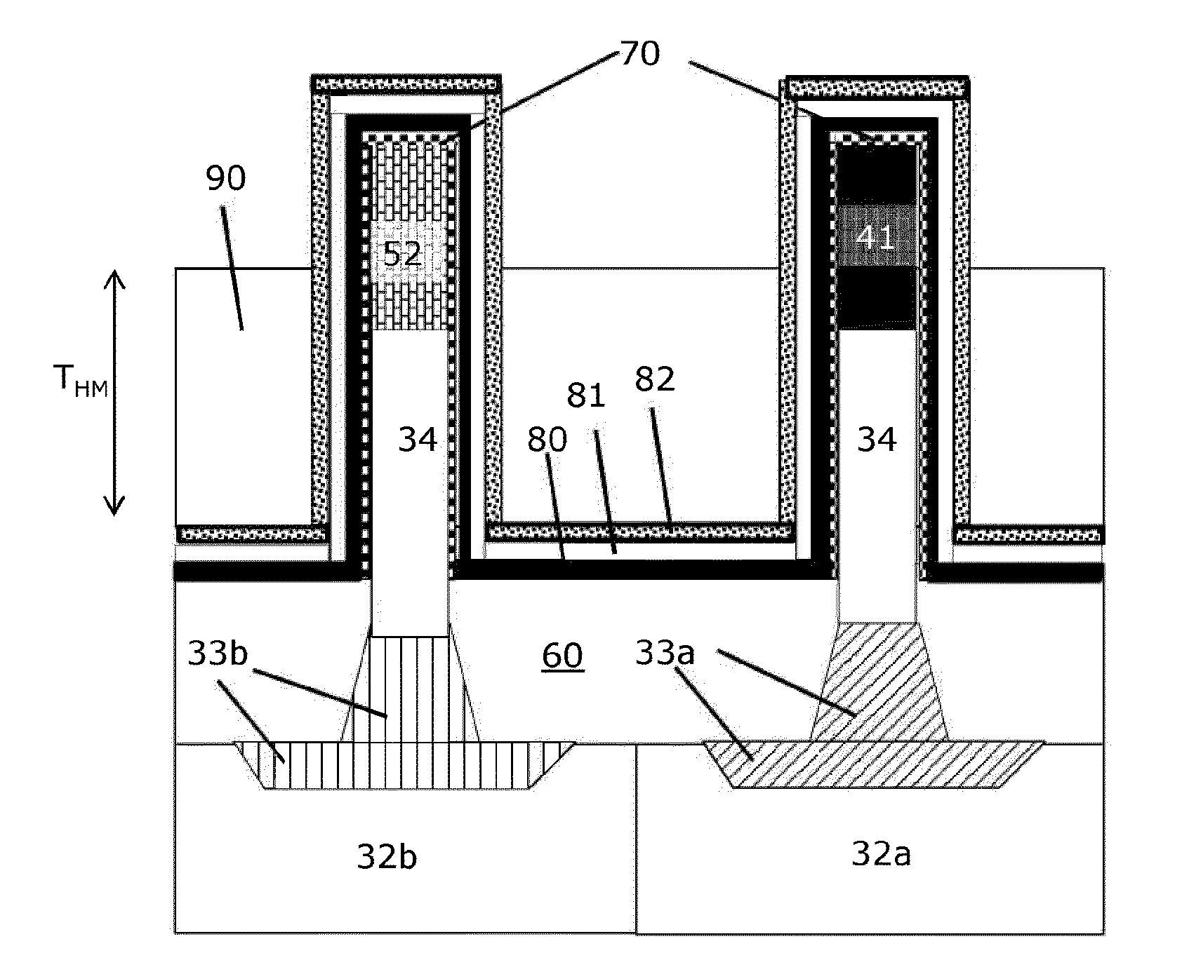
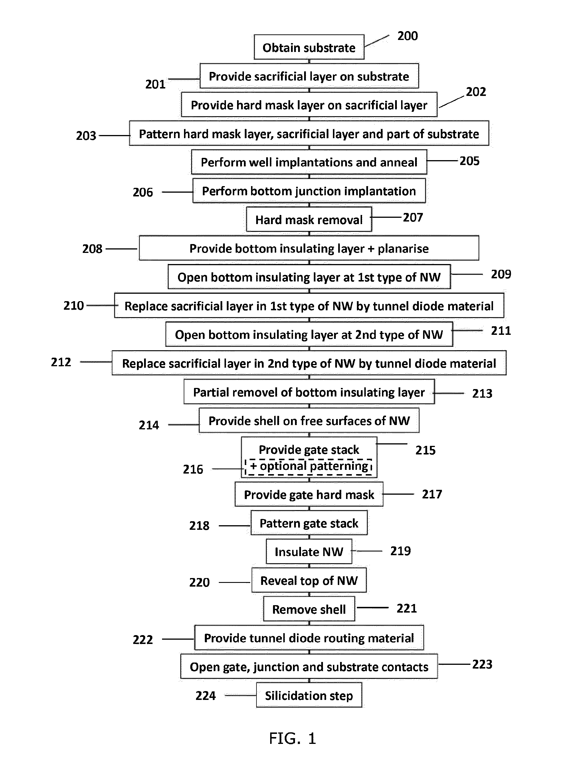
[0048]A method according to the present disclosure is schematically illustrated in a flowchart shown in FIG. 1 and is described in detail below. It has, however, to be understood that this is only an example of a suitable method for forming a device according to the disclosure, and that the sequence of the process steps as described hereinafter is not limiting the disclosure.

[0049]The method according to the first embodiment discloses the creation of a tunnel field effect transistor (TFET) having at least one nanowire (also referred to as NW-TFET), the nanowire comprising the channel region, source / drain regions, here called bottom and top junctions, and a heterosection. The heterosection is situated in between the channel region and one of the source / drain regions.

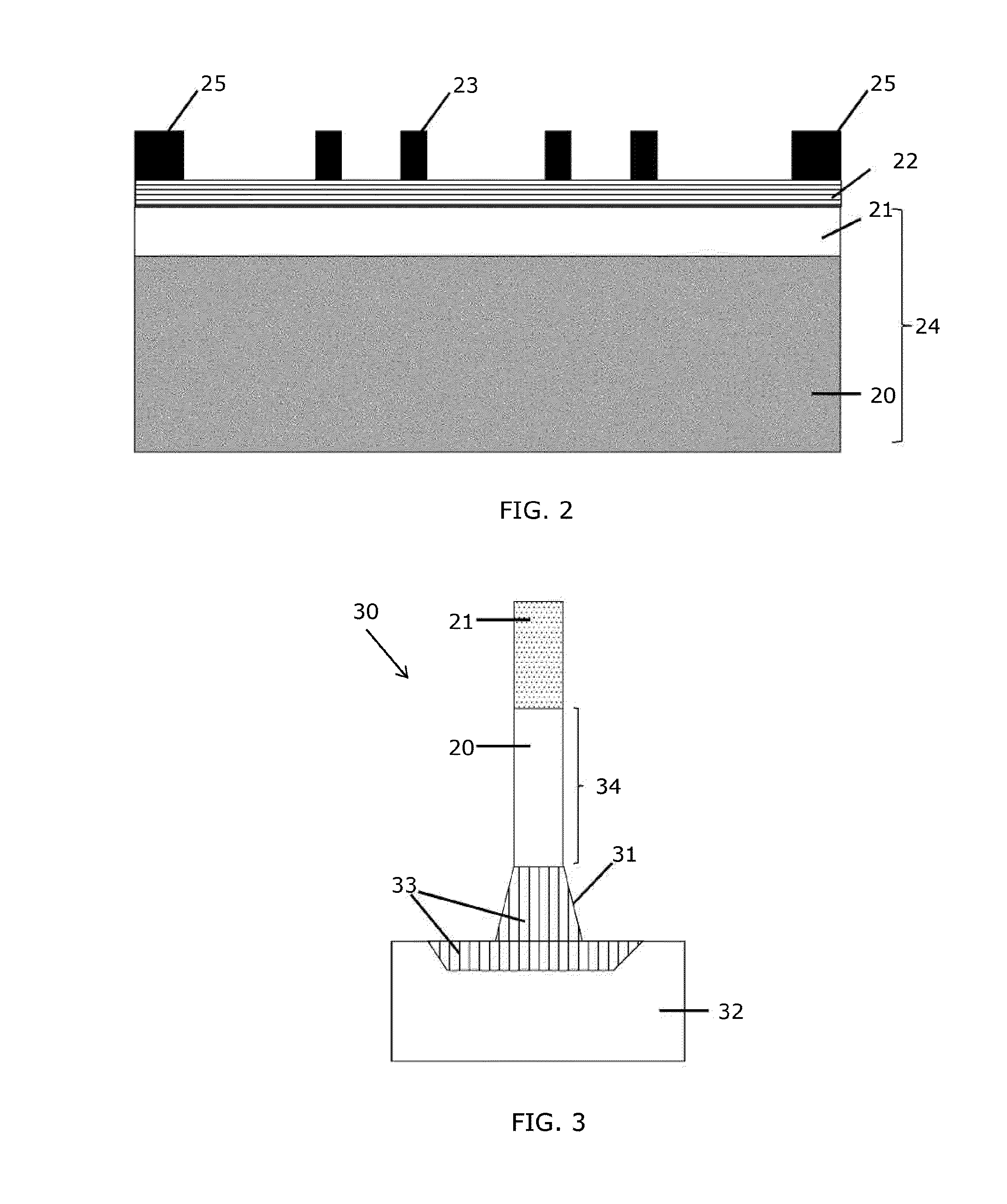
[0050]In a first step 200, a substrate 20 is provided. Preferably the substrate 20 is a semiconductor substrate. In particular embodiments, the substrate can for example be a silicon substrate, a substrate of a group IV m...

second embodiment

[0089]A method according to the present disclosure is schematically illustrated in a flowchart shown in FIG. 18 and is described in detail below. It has, however, to be understood that this is only an example of a suitable method for forming a device according to the disclosure, and that the sequence of the process steps as described hereinafter is not limiting the disclosure.

[0090]A number of steps of this method according to the second embodiment of the disclosure are as in the method according to the first embodiment of the disclosure, and are therefore not disclosed here in as much detail as above. Details which are lacking in the description of the second embodiment can be taken from the description of the first embodiment. A major difference between a method according to the first embodiment and a method according to the second embodiment is that in the first embodiment the heterojunction is formed at the beginning of the manufacturing method, while in the second embodiment th...


PUM

PropertyMeasurementUnit
thicknessaaaaaaaaaa
thicknessaaaaaaaaaa
thicknessaaaaaaaaaa

Abstract

The present disclosure provides a method for manufacturing at least one nanowire Tunnel Field Effect Transistor (TFET) semiconductor device. The method comprises providing a stack comprising a layer of channel material with on top thereof a layer of sacrificial material, removing material from the stack so as to form at least one nanowire from the layer of channel material and the layer of sacrificial material, and replacing the sacrificial material in the at least one nanowire by heterojunction material. A method according to embodiments of the present disclosure is advantageous as it enables easy manufacturing of complementary TFETs.

Description

CROSS-REFERENCE TO RELATED APPLICATION[0001]This application claims the benefit under 35 U.S.C. §119(a)-(d) of European application No. 10160382.7, filed Apr. 19, 2010, the disclosure of which is hereby expressly incorporated by reference in its entirety and is hereby expressly made a portion of this application.FIELD[0002]The present disclosure relates to the field of semiconductor devices and nanotechnology. More specifically, the disclosure relates to a nanostructure semiconductor device, more specifically a tunnel field effect transistor having a heterostructure nanowire, and a method for manufacturing such tunnel field effect transistor devices with integrated nanowires. In particular the present disclosure relates to a method for manufacturing complementary vertical TFETS, and to complementary TFETs thus obtained.BACKGROUND[0003]Microelectronic devices are generally fabricated on semiconductor substrates as integrated circuits. A complementary metal-oxide-semiconductor (CMOS) ...

Claims


Application Information

Patent Timeline
Patent Type & Authority Patents(United States)
IPC IPC(8): H01L21/84
CPCB82Y10/00H01L29/0665H01L29/7391H01L29/66356H01L29/267H01L29/165H01L21/823885
Inventor ROOYACKERS, RITALEONELLI, DANIELEVANDOOREN, ANNEVERHULST, ANNE S.LOO, ROGERDE GENDT, STEFAN
Owner INTERUNIVERSITAIR MICRO ELECTRONICS CENT (IMEC VZW)
Learn More