
Magnetic semiconductor material

a semiconductor material and semiconductor technology, applied in the field of magnetic semiconductor materials, can solve the problems of not having a suitable pn homojunction magnetic device, and not being able to meet the requirements of practical us

Inactive Publication Date: 2013-04-16
JAPAN SCI & TECH CORP
View PDF6 Cites 4 Cited by
  • Summary
  • Abstract
  • Description
  • Claims
  • Application Information

AI Technical Summary

Benefits of technology

The compound achieves bipolar conduction and high magnetic transition temperatures, enabling the formation of magnetic pn homojunction structures suitable for advanced magnetic devices, including sensors and memory elements.

Problems solved by technology

Furthermore, Cr3+ having a 3d6 electron configuration disadvantageously exhibits a magnetic moment smaller than and a Curie temperature (150 K) lower than those of the 3d5 electron configuration of the Mn2+ ion and the Fe3+ ion.
Due to these drawbacks, a pn homojunction magnetic device suitable for practical use has not been available.
These devices are named spin bipolar devices but are not put to practical use because formation of high-quality pn junction structures is difficult and the magnetic transition temperature of the magnetic semiconductor is lower than room temperature.Nonpatent document 1: P. W. Cheng et al.

Method used


Image

  • Magnetic semiconductor material
  • Magnetic semiconductor material
  • Magnetic semiconductor material

Examples


example 1

Example 1-1

Synthesis of LaMnOP:Ca and Magnetic and Electrical Properties

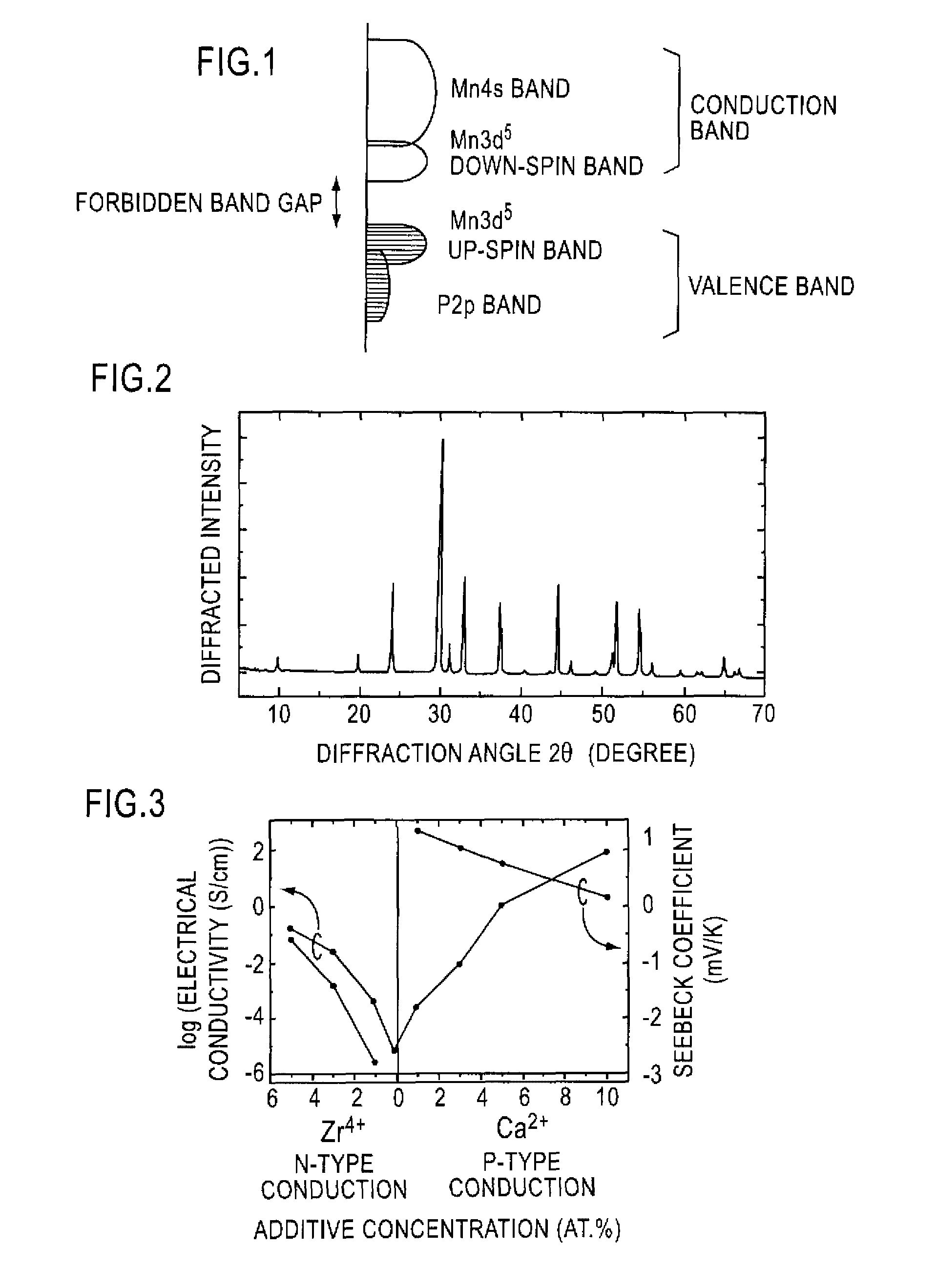
[0043]To a mixture powder of LaP and MnO at a chemical equivalent ratio, about 1 at. % of LaP2 was added such that the P was in excess of the stoichiometric composition. Furthermore, metallic Ca was added in an amount of 0 at. % (Sample 1), 3 at. % (Sample 2), and 10 at. % (Sample 3) relative to lanthanum, and the resulting mixture was retained at 1100° C. for 10 hours in an argon gas atmosphere and gradually cooled to obtain a gray powder sample. FIG. 2 showing the X-ray diffraction spectrum of each resulting powder demonstrates that all powder samples were LaMnOP compounds having an impurity content of less than 1 percent by mass.

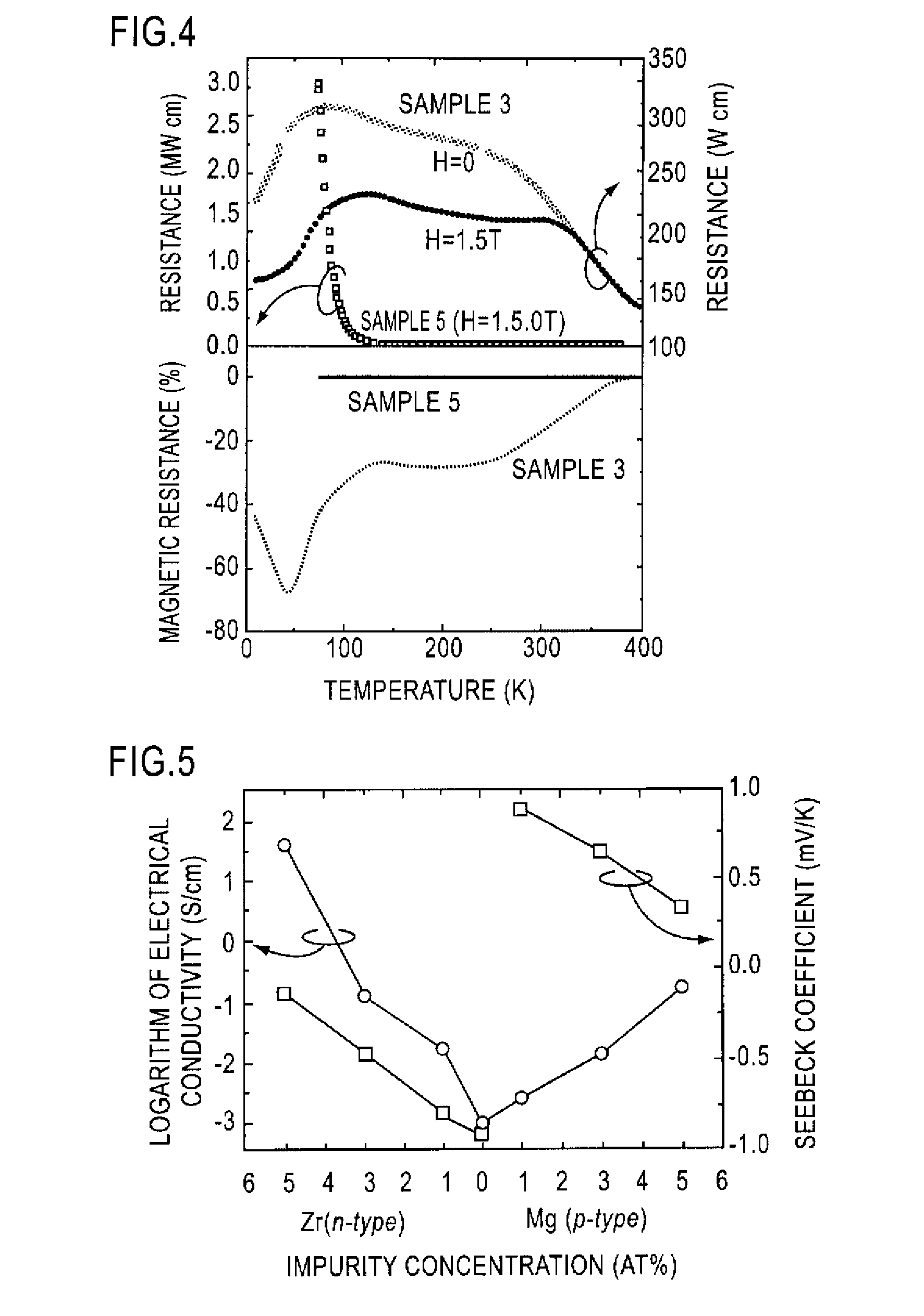
[0044]The dependency of the magnetic moment (M) on magnetic field (H=0 to 7 T) and temperature (T=4 K to 400 K) of each of Samples 1, 2, and 3 were measured with a sample oscillating magnetometer. At a temperature lower than the magnetic transition temperature, M rapidly increases by ...

example 1-2

Synthesis of LaMnOP:Zr and Electrical and Magnetic Properties

[0046]To a mixture powder of LaP and MnO at a chemical equivalent ratio, metallic Zr was added in an amount of 1 at. % (Sample 4), 3 at. % (Sample 5), and 5 at. % (Sample 6) relative to lanthanum, and the resulting mixture was retained at 1200° C. for 12 hours in an argon gas atmosphere and gradually cooled to obtain a gray powder sample. An X-ray diffraction spectrum of the resulting powder demonstrated that all powder samples were LaMnOP compounds having an impurity content of less than 1 percent by mass.

[0047]The dependency of magnetic moment (M) on magnetic field (H=0 to 7 T) and temperature (T=4 K to 400 K) of each of Samples 4, 5, and 6 was measured with a sample oscillating magnetometer. Although Ms appeared at low temperature for Samples 4 and 5, Ms did not appear before 0 K for Sample 6. The value of Ms was less than 0.3 μB per Mn2+ ion. When the reciprocal of the magnetic susceptibility is plotted versus absolute...

example 2

Synthesis of LaMnOAs:Mg or Zr and Electrical and Magnetic Properties

[0049]A powder in which LaAs and MnO were mixed at a chemical equivalent ratio was retained at 1100° C. for 10 hours in an argon gas atmosphere and gradually cooled to obtain a gray powder sample. A powder X-ray spectrum of the resulting sample showed that the resulting powder was a layered LaMnOAs compound phase having a ZrCuSiAs-type crystal structure in the space group P4 / nmm, and that the impurity phase contained therein was less than 1 percent by mass.

[0050]To a mixture powder of LaAs and MnO at a chemical equivalent ratio, metallic Mg was added in an amount of 1 at. % (Sample 7), 3 at. % (Sample 8), and 5 at. % (Sample 9) relative to lanthanum, and the resulting mixture was retained at 1100° C. for 10 hours in a reducing atmosphere containing hydrogen gas and gradually cooled to obtain a gray powder sample. A powder X-ray spectrum of the resulting sample showed that the resulting powder was a layered LaMnOAs c...


PUM

PropertyMeasurementUnit
temperatureaaaaaaaaaa
electrical conductivityaaaaaaaaaa

Abstract

A magnetic semiconductor material contains at least one type of transition metals (Mn2+, Fe3+, Ru3+, Re2+, and Os3+) having five electrons in the d atomic orbital as a magnetic ion, in which the magnetic semiconductor material exhibits n-type electrical conduction by injection of an electron carrier and p-type electric conduction by injection of a hole carrier. A specific example is a layered oxy-pnictide compound represented by LnMnOPn (wherein Ln is at least one type selected from Y and rare earth elements of La, Ce, Pr, Nd, Sm, Eu, Gd, Tb, Dy, Ho, Er, Tm, Yb, and Lu, and Pn is at least one selected from pnicogen elements of N, P, As, Bi, and Sb). A high-sensitivity magnetic sensor, current sensor, or memory device can be made by using a magnetic pn homojunction structure made of thin films composed of the magnetic semiconductor material.

Description

TECHNICAL FIELD[0001]The present invention relates to a magnetic semiconductor material, which is a single compound capable of exhibiting two different conductivity types, i.e., n-type and p-type. In particular, it relates to a magnetic semiconductor material including an oxy-pnictide layered compound.BACKGROUND ART[0002]A magnetic semiconductor compound is a unique compound having both semiconducting electrical property and magnetic property. Because the magnetic semiconductor compound exhibits a large magnetoresistive effect near the magnetic transition temperature (Curie temperature Tc or Neel temperature TN), its application to magnetic sensors and the like are expected. However, most magnetic semiconductor compounds discovered so far exhibit only one conductivity type, i.e., either n-type or p-type, and no magnetic semiconductor compound that can exhibit both conductivity types, i.e., n-type and p-type, has been discovered to date except for CdCr2Se4 (non-patent document 1).[00...

Claims


Application Information

Patent Timeline
Patent Type & Authority Patents(United States)
IPC IPC(8): B32B15/04
CPCC01G45/006C04B35/50H01F1/407H01F10/193Y10T428/325C01P2002/72C01P2002/76C01P2006/40C01P2006/42C04B2235/3224C04B2235/3225C04B2235/3234C04B2235/3262C04B2235/3294C04B2235/3298C04B2235/40C04B2235/42H01F1/0009C01P2002/52
Inventor HOSONO, HIDEOHIRANO, MASAHIROHIRAMATSU, HIDENORIKAMIYA, TOSHIOYANAGI, HIROSHIMOTOMITSU, EIJI
Owner JAPAN SCI & TECH CORP
Learn More