Apparatus and method for the production of flexible semiconductor devices

a semiconductor device and apparatus technology, applied in the direction of electrical equipment, chemical vapor deposition coatings, coatings, etc., can solve the problems of loss of interface steepness between two subsequent semiconductor layers, reduced device performance, and relative difficulty and cost of production apparatus adaptation, so as to achieve the maximum productivity level, easy to adapt, and high device performance

Inactive Publication Date: 2013-05-14
VHF TECH
View PDF27 Cites 1 Cited by
  • Summary
  • Abstract
  • Description
  • Claims
  • Application Information

AI Technical Summary

Benefits of technology

[0013]The apparatus according to the present invention is easily adaptable as it allows independent tuning of all production parameters, in particular substrate speed through the reaction region, from one deposition phase to the next. Furthermore, with the use of the production is method according to the present invention, different type of devices, i.e. p-i-n, n-i-p, double and triple stacked cells as well as thin film transistors (TFT) can be produced on the same apparatus, without implying modification of the production apparatus and at an always maximal productivity level. As there is no interrelation at all between the parameters of each individual layer deposited, no compromise needs to be found between the deposition conditions of each layer. Higher performance devices with steeper interface between neighboring layers can therefore be achieved.
[0014]The deposition gas diffusion issues can be avoided thanks to the possible use of a unique deposition chamber for the production of any flexible multi-layer semiconductor device and, for the same reason, the cost of the production apparatus according to the invention is significantly lower than the cost of a roll-to-roll apparatus as described in the prior art.
[0015]The roll-to-roll production apparatus according to the invention and the related production method also permit fast production processes fully compatible with mass-production conditions.

Problems solved by technology

If the variation of the thickness ratio cannot be compensated by a change in the relative reactive gas concentrations, the manufacture of other semiconductor devices having differing relative dimensions might require changing the relative chamber lengths, which can mean a relatively difficult and costly adaptation of the production apparatus.
Another drawback of such production apparatuses is the complex isolation systems needed to prevent reaction gases from diffusing from one deposition chamber to the next, in order to avoid cross-contamination from one layer to the next, which would result, on the manufactured device, in a loss of interface steepness between two subsequent semiconductor layers, hence in lower device performance.
A first disadvantage of this method is that, given the relatively small deposition surface, these purge cycles notably decrease the overall productivity of a given apparatus.
A further disadvantage is that the surface of the last deposited semiconductor layer is not protected during the purge cycle, thus altering and possibly deteriorating the properties of its interface to the next layer.
In the context of thin film silicon solar cell manufacturing, the doping cross-contamination, particularly between a first doped and a subsequent intrinsic layer, is the most critical issue and requires therefore long and complex purge cycles or complex isolation systems depending on the configuration of the semiconductor production apparatus.

Method used


Image

  • Apparatus and method for the production of flexible semiconductor devices
  • Apparatus and method for the production of flexible semiconductor devices
  • Apparatus and method for the production of flexible semiconductor devices

Examples


Embodiment Construction

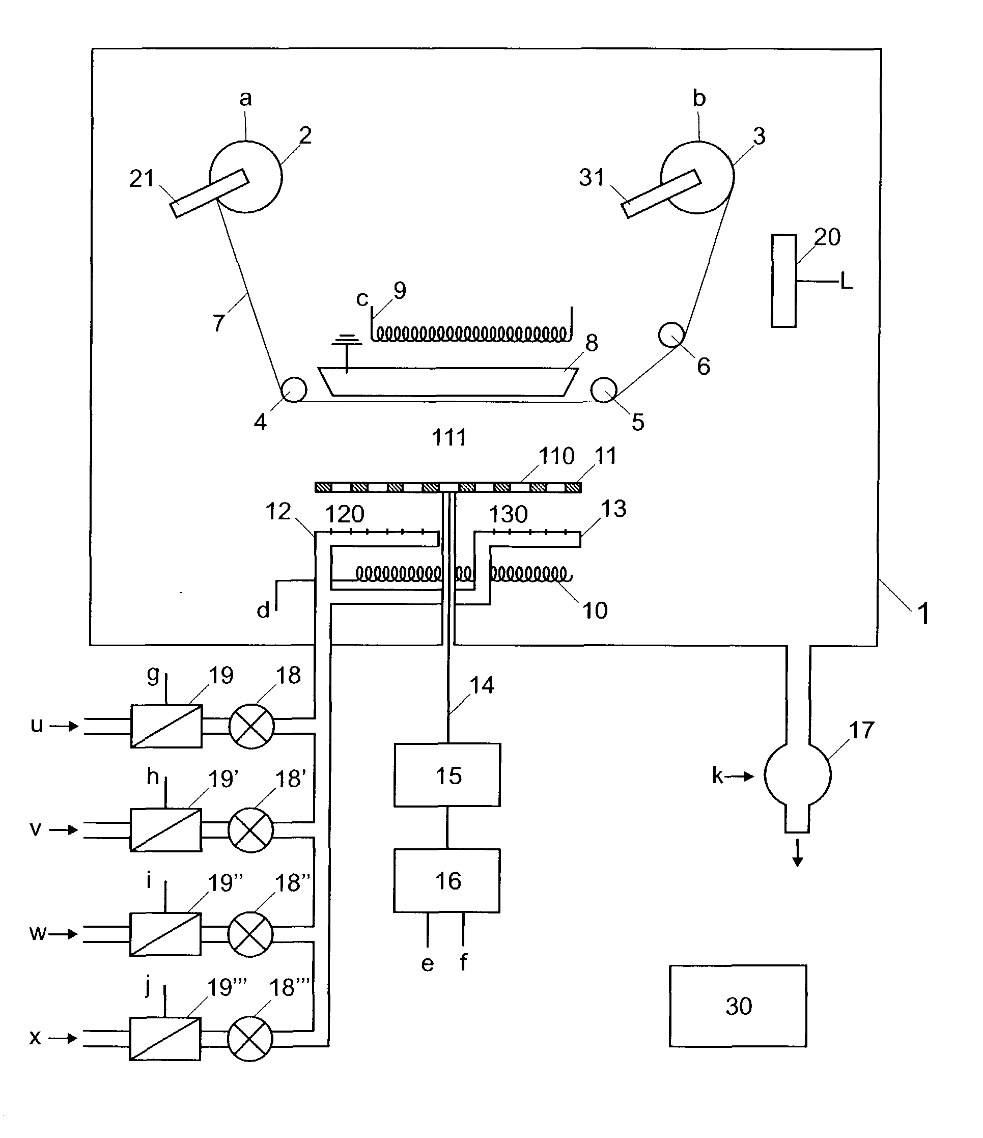
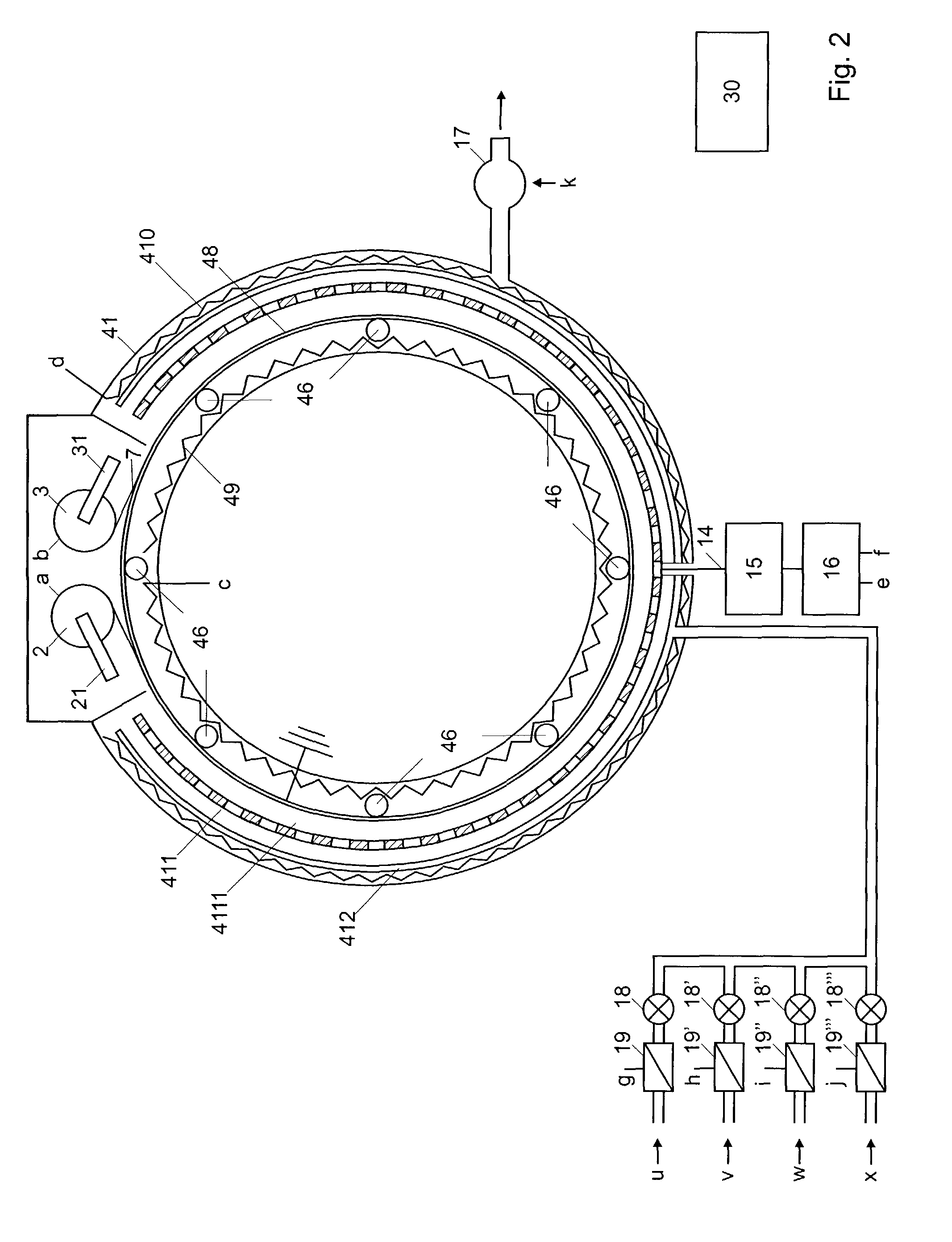
[0022]The apparatus according to the preferred embodiment of the present invention (FIG. 1) comprises one deposition chamber 1. A reaction region 111 within the deposition chamber is determined by the space between an electrode 11 and a grounded slide shoe 8. The electrode 11 is connected to an radio-frequency (RF) power generator 16 through an RF line 14, allowing the application of an electromagnetic power on the electrode 11 creating an electrical field in the reaction region 111. An impedance adaptor 15 placed between the RF power generator 16 and the RF line 14 prevents undesired reflections on the RF line 14. The power level e and the frequency f of the generated electromagnetic power can be controlled by a computer program product running on a controller 30. Two manifolds 12,13 allow a regular introduction of gas into the reaction region 111 through their apertures 120, 130 and apertures 110 in the electrode 11. Four valves 18, 18′, 18″, 18′″ control the introduction of diffe...


PUM

PropertyMeasurementUnit
flexibleaaaaaaaaaa
electromagnetic poweraaaaaaaaaa
frictionaaaaaaaaaa

Abstract

Apparatus for continuously producing flexible semiconductor devices through deposition of a plurality of semiconductor layers onto a moving flexible substrate by using Plasma Enhanced Chemical Vapor Deposition (PECVD) processing, where at least two successive layers are deposited in the same deposition chamber onto the substrate traveling in opposite directions. Computer program product directly loadable into the internal memory of a digital computer comprising software code portions for determining and controlling all the necessary parameters for the production of flexible semi-conductor devices in a such apparatus when said computer program product is run on a computer. Roll-to-roll method for producing flexible semiconductor devices, wherein a plurality of semiconductor layers are deposited in the same deposition chamber onto a flexible substrate moving in opposite directions. Flexible semiconductor device produced with said method, where the penetration rate of one semiconductor layer into its neighboring layer is remarkably low.

Description

[0001]This application claims priority of European Patent Application EP 02076056.7, the content of which is hereby incorporated.FIELD OF THE INVENTION[0002]The present invention relates to an apparatus for continuously producing flexible semiconductor devices through deposition of a plurality of semiconductor layers onto a moving flexible substrate by using Plasma Enhanced Chemical Vapor Deposition (PECVD) processing. The present invention also relates to a computer program product directly loadable into the internal memory of a digital computer comprising software code portions for controlling the production of flexible semi-conductor devices in an apparatus according to the invention when said computer program product is run on a computer. The present invention further relates to a roll-to-roll method for producing flexible semiconductor devices, wherein a plurality of semiconductor layers are deposited onto a moving flexible substrate, as well as to a flexible semiconductor devi...

Claims


Application Information

Patent Timeline
Patent Type & Authority Patents(United States)
IPC IPC(8): C23C16/00H01L21/306C23C16/509C23C16/52C23C16/54
CPCC23C16/509C23C16/52C23C16/545H01J37/32082H01J37/3277
Inventor FISCHER, DIEGOTORRES, PEDRO
Owner VHF TECH
Why Eureka
Try Eureka