Manufacturing method of microcrystalline silicon film and manufacturing method of thin film transistor

a manufacturing method and technology of microcrystalline silicon, applied in the direction of semiconductor devices, electrical appliances, basic electric elements, etc., can solve the problems of inability to clearly express moving images, inability to effectively express moving images, etc., to achieve improved adhesion and improve adhesion

Inactive Publication Date: 2013-05-14
SEMICON ENERGY LAB CO LTD +1
View PDF47 Cites 0 Cited by
  • Summary
  • Abstract
  • Description
  • Claims
  • Application Information

AI Technical Summary

Benefits of technology

[0015]In the above embodiment of the present invention, by performing the plasma treatment in an atmosphere including oxygen on the microcrystalline silicon grain, the silicon oxide grain having high crystallinity can be formed over the insulating film. Further, by forming the microcrystalline silicon film over the silicon oxide grain having high crystallinity, the adhesion force between the insulating film and the microcrystalline silicon film can be increased.

Problems solved by technology

However, under current moving image circumstances (e.g., 3D movies or 3D sports broadcast), it is difficult to clearly express moving images with liquid crystal televisions including amorphous silicon TFTs; accordingly, TFTs having high mobility that can respond at high speed are under development.
It is known that the field-effect mobility (μFE_sat.) of a thin film transistor in which only a microcrystalline silicon film is employed for a channel formation region is higher than that of an amorphous silicon TFT; however, the crystallization may proceed excessively and the off-leakage current (Ioff) may be increased in such a transistor.
Therefore, optimization of crystallinity is an issue.
In the case where a SiNx film is used as a gate insulating film of a thin film transistor and a microcrystalline silicon film serving as an active layer is formed over the SiNx film, the adhesion force between the microcrystalline silicon film and the SiNx film is low; as a result, a film bulge or film peeling tends to occur.
With such N2O plasma treatment, the adhesion between the microcrystalline silicon film and the SiNx film is somewhat improved but is still insufficient.

Method used


Image

  • Manufacturing method of microcrystalline silicon film and manufacturing method of thin film transistor
  • Manufacturing method of microcrystalline silicon film and manufacturing method of thin film transistor
  • Manufacturing method of microcrystalline silicon film and manufacturing method of thin film transistor

Examples


embodiment 1

[Embodiment 1]

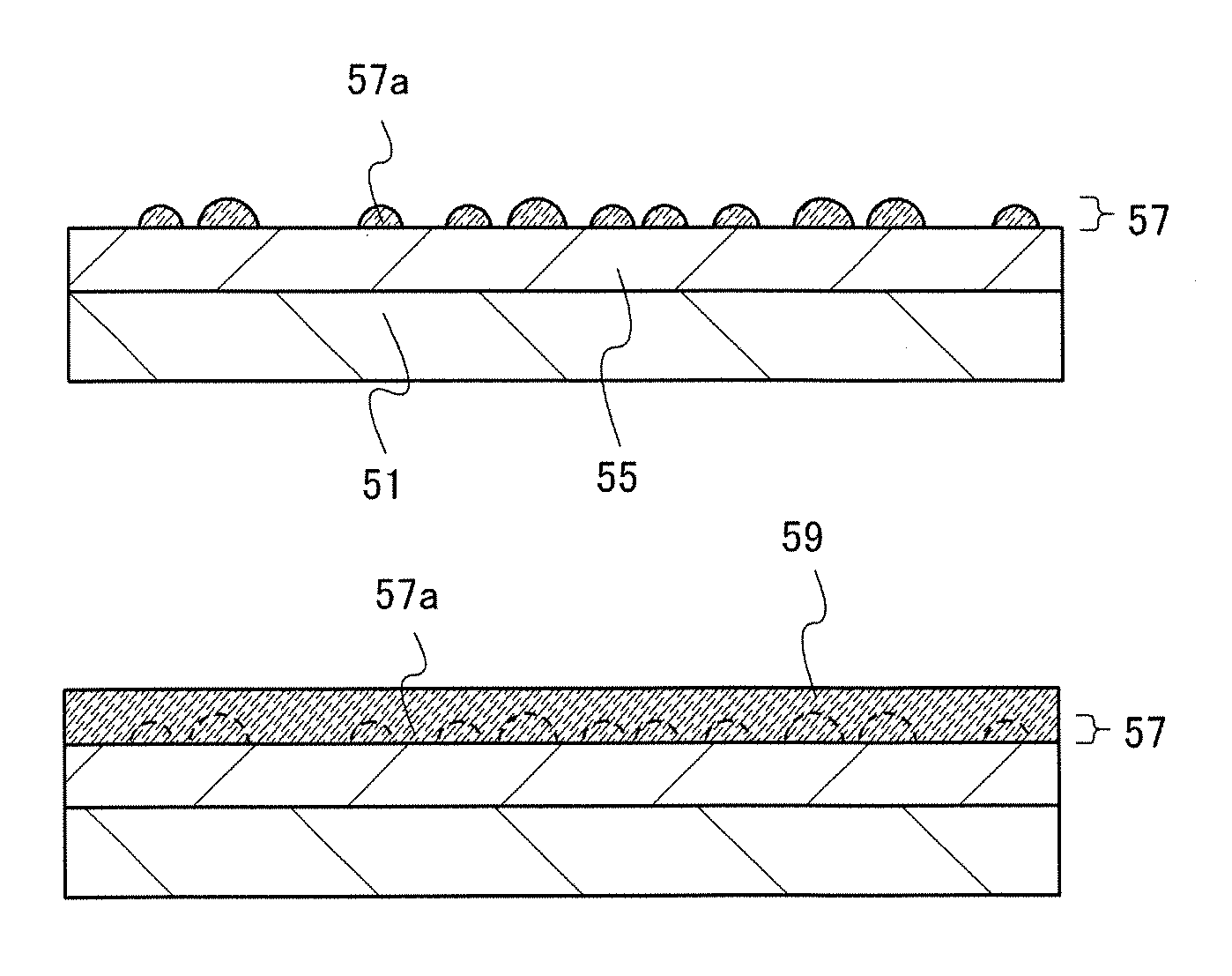
[0028]In this embodiment, a manufacturing method of a microcrystalline silicon film with improved adhesion between an insulating film and the microcrystalline silicon film will be described with reference to FIGS. 1A and 1B.

[0029]As illustrated in FIG. 1A, an insulating film 55 is formed over a substrate 51, and plasma treatment in an atmosphere including oxygen or plasma oxidation is performed on a surface of the insulating film 55. Next, a microcrystalline silicon grain having a height that allows the microcrystalline silicon grain to be completely oxidized by later plasma oxidation or the like (e.g., a height greater than 0 nm and less than or equal to 5 nm) is formed over the insulating film 55 by a plasma CVD method, and the microcrystalline silicon grain is subjected to plasma treatment in an atmosphere including oxygen or plasma oxidation; thus, a silicon oxide grain 57a having high crystallinity is formed over the insulating film 55. As the plasma treatment in ...

embodiment 2

[Embodiment 2]

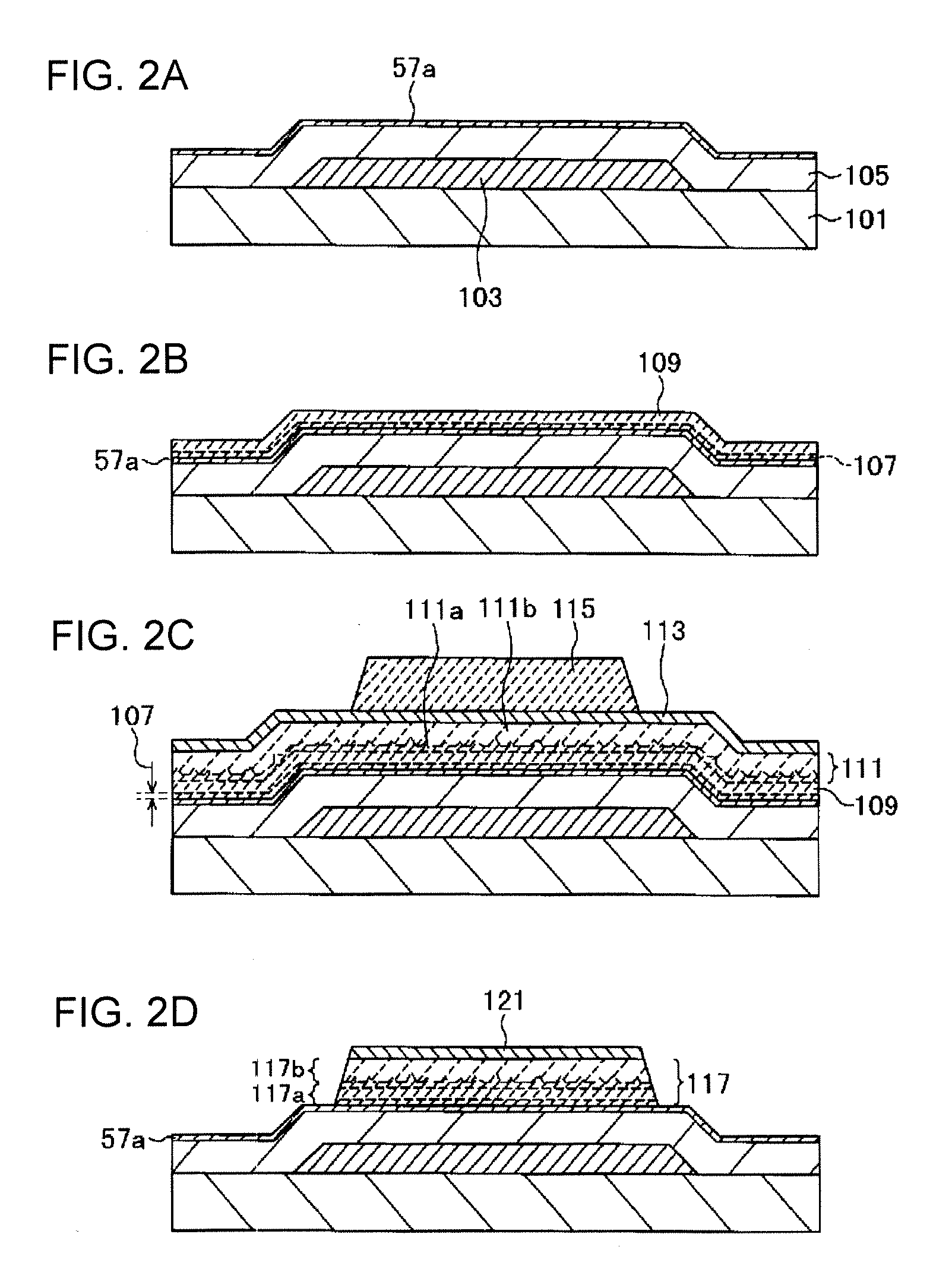
[0045]In this embodiment, a manufacturing method of a thin film transistor formed in a semiconductor device according to one embodiment of the present invention will be described with reference to FIGS. 2A to 2D, FIGS. 3A and 3B, and FIGS. 4A to 4C. Note that an n-channel thin film transistor has higher carrier mobility than a p-channel thin film transistor. In this embodiment, a manufacturing method of an n-channel thin film transistor will be described.

[0046]As illustrated in FIG. 2A, a gate electrode 103 is formed over a substrate 101. Then, a gate insulating film 105 which is formed of a silicon nitride film (a SiNx film) and covers the gate electrode 103 (hereinafter also referred to as a first gate electrode) is formed, and N2O plasma treatment is performed on a surface of the gate insulating film 105. Next, a microcrystalline silicon grain having a height that allows the microcrystalline silicon grain to be completely oxidized by later plasma oxidation or the li...

embodiment 3

[Embodiment 3]

[0104]In this embodiment, a manufacturing method of a thin film transistor formed in a semiconductor device that is an embodiment of the present invention will be described with reference to FIG. 5. FIG. 5 corresponds to the step illustrated in FIG. 4B.

[0105]In a manner similar to that of Embodiment 2, a conductive film 127 is formed through the process of FIGS. 2A to 2D and FIG. 3A.

[0106]Then, as illustrated in FIG. 5, wirings 129a and 129b are formed and an impurity silicon film 121 and a silicon stacked body 117 are partly etched, so that a pair of impurity silicon films 131a and 131b serving as a source region and a drain region are formed in a manner similar to that of Embodiment 2. A silicon stacked body 143 including a microcrystalline silicon region 143a and a region 143b in which crystallization is suppressed is formed. At this time, the silicon stacked body 117 is etched so as to expose the region 143b in which crystallization is suppressed, so that the silic...


PUM

PropertyMeasurementUnit
temperatureaaaaaaaaaa
thicknessaaaaaaaaaa
heightaaaaaaaaaa

Abstract

An object is to provide a manufacturing method of a microcrystalline silicon film with improved adhesion between an insulating film and the microcrystalline silicon film. The microcrystalline silicon film is formed in the following manner. Over an insulating film, a microcrystalline silicon grain having a height that allows the microcrystalline silicon grain to be completely oxidized by later plasma oxidation (e.g., a height greater than 0 nm and less than or equal to 5 nm), or a microcrystalline silicon film or an amorphous silicon film having a thickness that allows the microcrystalline silicon film or the amorphous silicon film to be completely oxidized by later plasma oxidation (e.g., a thickness greater than 0 nm and less than or equal to 5 nm) is formed. Plasma treatment in an atmosphere including oxygen or plasma oxidation is performed on the microcrystalline silicon grain, the microcrystalline silicon film, or the amorphous silicon film, so that a silicon oxide grain or a silicon oxide film is formed over the insulating film. A microcrystalline silicon film is formed over the silicon oxide grain or the silicon oxide film.

Description

TECHNICAL FIELD[0001]The present invention relates to a manufacturing method of a microcrystalline silicon film and a manufacturing method of a thin film transistor.BACKGROUND ART[0002]For conventional liquid crystal televisions, amorphous silicon TFTs (thin film transistors) are used in many cases and recognized as structures that can be relatively easily manufactured in terms of manufacturing cost.[0003]However, under current moving image circumstances (e.g., 3D movies or 3D sports broadcast), it is difficult to clearly express moving images with liquid crystal televisions including amorphous silicon TFTs; accordingly, TFTs having high mobility that can respond at high speed are under development. For this reason, a microcrystalline silicon film has been developed.[0004]It is known that the field-effect mobility (μFE_sat.) of a thin film transistor in which only a microcrystalline silicon film is employed for a channel formation region is higher than that of an amorphous silicon T...

Claims


Application Information

Patent Timeline
Patent Type & Authority Patents(United States)
IPC IPC(8): H01L21/20H01L21/36
CPCH01L21/02488H01L21/02502H01L21/02532H01L21/0262H01L21/02658H01L21/32105H01L29/04H01L29/66765H01L29/78678H01L29/78696
Inventor MIYAIRI, HIDEKAZUIENAGA, TAKASHIMORIGUCHI, MASAOKANZAKI, YOSUKE
Owner SEMICON ENERGY LAB CO LTD
Why Eureka
Try Eureka