Method and apparatus for increasing local plasma density in magnetically confined plasma

a magnetically confined plasma and density technology, applied in vacuum evaporation coatings, electric discharge tubes, coatings, etc., can solve the problems of easy damage to exposed dielectric materials, microtrenching damage, and difficult to perform resputtering without exposing dielectric layers to plasma, so as to reduce the reliability of formed ic devices, reduce the adhesion of subsequently deposited layers, and easy to become damaged

Active Publication Date: 2013-05-28
NOVELLUS SYSTEMS
View PDF199 Cites 9 Cited by
  • Summary
  • Abstract
  • Description
  • Claims
  • Application Information

AI Technical Summary

Benefits of technology

[0005]With an ongoing miniaturization of IC devices, especially with processing of devices at a 65 nm technology node and at more advanced nodes, it became more challenging to perform resputtering without exposing dielectric layers to plasma. It was noted that a layer of dielectric can become exposed during resputter, especially when large amounts of diffusion barrier or other material are removed from the wafer substrate. When resputtering is performed under conventional conditions, the exposed dielectric material can easily become damaged by high-energy ions that impinge upon it. One type of such damage is microtrenching, which manifests itself in increased dielectric etching at particular locations within the recessed features of the wafer. In one typical example, microtrenches are formed in the proximity of the sidewalls in the bottom portions of the recessed features, e.g., in the trench bottoms. Microtrenching leads to decreased reliability of the formed IC devices due to reduced adhesion of the subsequently deposited layers. Further, microtrenching contributes to an increase in line-to-line leakage due to local increase in current densities in the microtrenches. It was therefore recognized that there is a need for a resputtering method that would remove material from the wafer surface without causing microrotrenching in the exposed dielectric layer.
[0006]Efficient resputtering of diffusion barrier layers in the presence of exposed dielectric can be achieved when higher density plasma is employed. Microtrenching can be substantially eliminated when resputtering is performed using a high flux of low energy ions at the wafer surface. For example, an ion flux of at least about 5·1015 ions / cm2 s, preferably of at least about 1016 ions / cm2 s, having a mean energy of less than about 250 eV, preferably less than about 200 eV, e.g., less than about 150 eV is effective for diffusion barrier material etching without causing microtrenching in many types of low-k dielectrics. It is understood that different types of dielectric materials may have different susceptibility to plasma damage, and that lower energy plasma may be needed to avoid microtrenching in more delicate dielectrics, while higher energy plasma may be tolerated by more robust dielectric materials. Without being bound by a particular theory of operation, it is believed that lower kinetic energy of the ions contacting the wafer leads to decreased dielectric damage, while the higher density of ion flux increases the etch rate and maximizes resputtering efficiency.
[0007]High ion flux of low-energy ions can be produced in one embodiment by generating a high-density low ion energy plasma proximate the wafer substrate. Conventionally, generation of plasma having a density of greater than about 1011 electrons / cm3 proximate the wafer substrate, proved to be difficult to achieve. Therefore, high ion fluxes needed for resputtering in low energy regime, could not be easily attained. Further, as higher density plasmas were generated, the radial uniformity of an ion flux across the wafer diminished, resulting in higher rates of material removal at the center of the wafer compared to wafer edges. It was recognized that new methods and apparatus for increasing local plasma density and for improving plasma uniformity were needed.
[0008]According to some embodiments presented herein, plasma density of at least about 5·1011 electrons / cm3 (or ions / cm3), preferably at least about 1012 electrons / cm3 and, in some cases, as high as at least about 1013 electrons / cm3 is achieved in the vicinity of the wafer surface (e.g., within about 3 cm of the wafer surface, such as within 1 cm of the wafer surface). Increased ion flux provided by such plasma achieves efficient etching of diffusion barrier or other material, even when the kinetic energy of ions in the plasma is relatively low.
[0010]While methods and apparatus described herein address the microtrenching problem by providing high density low energy plasmas at the wafer surface, the described methods and apparatus are not limited to this particular application. In general, these methods can be used for increasing local plasma density in a variety of processes, including both resputtering (in a low energy and high energy regimes) and deposition. While provided methods are particularly suitable for resputtering in a low-energy regime, in those instances when dielectric is not exposed during resputtering, higher energy plasmas may be used to increase the etching rates. In yet other embodiments provided methods may be used for depositing diffusion barrier and seed layer materials. When high density low ion energy plasmas are used during deposition, the quality of deposited films can improve, due to decreased incorporation of inert gas ions into deposited films. In yet other embodiments provided methods are used to generate plasmas, that do not necessarily have high density, but have higher density than they would otherwise have in a conventional apparatus.
[0019]In those embodiments, where the plasma in the second plasma region is further magnetically confined, it is often preferable to increase plasma density in the second plasma region using a combination of electric and magnetic fields. In one embodiment the E vector (characterizing the electric field generated by the positively biased ion extractor) and the B vector (characterizing the magnetic field in the second plasma confinement region) are substantially orthogonal at least at one location. The generated electromagnetic forces further accelerate the trapped electrons in this region and produce a region of higher density plasma. In one implementation, the formed plasma is toroidally shaped above the wafer, and contributes to non-uniformity improvement at the wafer edges.

Problems solved by technology

With an ongoing miniaturization of IC devices, especially with processing of devices at a 65 nm technology node and at more advanced nodes, it became more challenging to perform resputtering without exposing dielectric layers to plasma.
When resputtering is performed under conventional conditions, the exposed dielectric material can easily become damaged by high-energy ions that impinge upon it.
One type of such damage is microtrenching, which manifests itself in increased dielectric etching at particular locations within the recessed features of the wafer.
Microtrenching leads to decreased reliability of the formed IC devices due to reduced adhesion of the subsequently deposited layers.
Further, microtrenching contributes to an increase in line-to-line leakage due to local increase in current densities in the microtrenches.
Conventionally, generation of plasma having a density of greater than about 1011 electrons / cm3 proximate the wafer substrate, proved to be difficult to achieve.
Therefore, high ion fluxes needed for resputtering in low energy regime, could not be easily attained.

Method used


Image

  • Method and apparatus for increasing local plasma density in magnetically confined plasma
  • Method and apparatus for increasing local plasma density in magnetically confined plasma
  • Method and apparatus for increasing local plasma density in magnetically confined plasma

Examples


Embodiment Construction

Introduction and Terminology

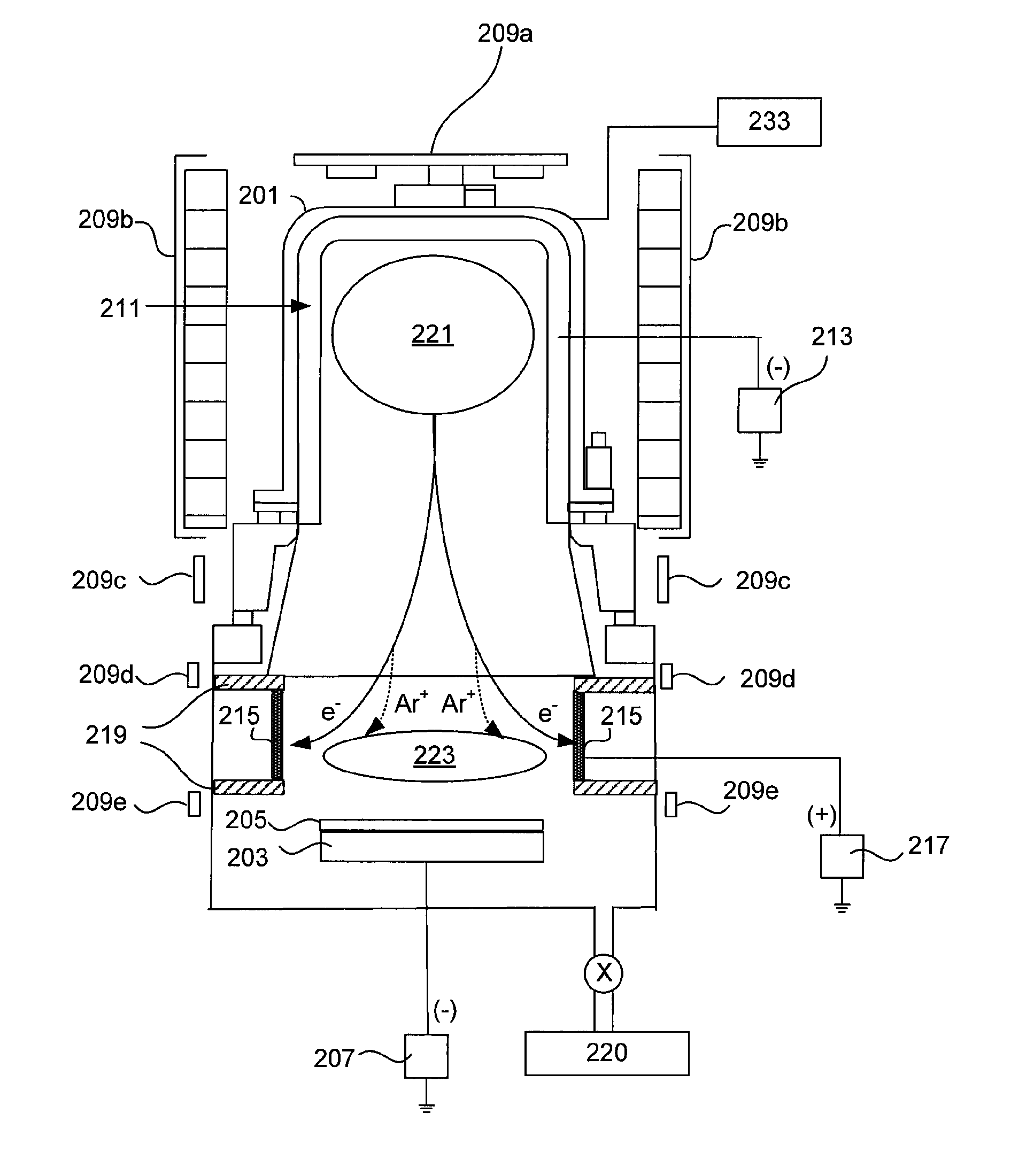
[0034]As mentioned, methods and apparatus for increasing local plasma density (e.g., plasma density proximate the substrate in a process chamber) are herein provided. The methods can be used, for example, in PVD and plasma pre-clean reactors that have at least one region of magnetically confined or shaped plasma. A greater than about two-fold, a five-fold and, in some embodiments, a ten-fold increase in local plasma density can be achieved by implementing provided methods. In some embodiments, provided methods are used to generate a high density plasma (e.g., a plasma having a density of at least about 1011 electrons / cm3, preferably at least about 1012 electrons / cm3 and in some cases at least about 1013 electrons / cm3) proximate the semiconductor wafer substrate, however the methods are not limited that way. For example, medium and low density plasmas may also be formed by increasing the density of even lower density plasmas.

[0035]Provided methods also inc...


PUM

PropertyMeasurementUnit
mean energyaaaaaaaaaa

Abstract

Local plasma density, e.g., the plasma density in the vicinity of the substrate, is increased by providing an ion extractor configured to transfer ions and electrons from a first region of magnetically confined plasma (typically a region of higher density plasma) to a second region of plasma (typically a region of lower density plasma). The second region of plasma is preferably also magnetically shaped or confined and resides between the first region of plasma and the substrate. A positively biased conductive member positioned proximate the second region of plasma serves as an ion extractor. A positive bias of about 50-300 V is applied to the ion extractor causing electrons and subsequently ions to be transferred from the first region of plasma to the vicinity of the substrate, thereby forming higher density plasma. Provided methods and apparatus are used for deposition and resputtering.

Description

CROSS-REFERENCE TO RELATED APPLICATIONS[0001]This application is a divisional application claiming priority from U.S. patent application Ser. No. 11 / 807,182 filed May 24, 2007, titled “Method and Apparatus for Increasing Local Plasma Density in Magnetically Confined Plasma”, naming Pradhan et al. as inventors, now U.S. Pat. No. 7,922,880, issued Apr. 12, 2011, which is incorporated herein by reference in its entirety for all purposes.FIELD OF THE INVENTION[0002]The present invention pertains to methods and apparatus for increasing local plasma density in magnetically confined plasma. In particular, the present invention pertains to plasma physical vapor deposition and sputter etching. The methods are particularly useful for sputter etching diffusion barrier layers and copper seed layers. The methods can also be applied for sputter etch back of other wafer materials, such as conductive lines.BACKGROUND OF THE INVENTION[0003]Miniaturization of integrated circuit (IC) devices demands s...

Claims


Application Information

Patent Timeline
Patent Type & Authority Patents(United States)
IPC IPC(8): H01L21/311C23C14/35C23F1/00
CPCC23C14/351H01J37/3266H01J37/3405H01J37/3461
Inventor PRADHAN, ANSHU A.HAYDEN, DOUGLAS B.KINDER, RONALD L.DULKIN, ALEXANDER
Owner NOVELLUS SYSTEMS
Why Eureka
Try Eureka