

Method for manufacturing insulated gate field effect transistor
a technology of field effect transistor and insulated gate, which is applied in the direction of transistors, electrical devices, semiconductor devices, etc., can solve the problems of deterioration of the characteristics of the insulated gate field effect transistor, and achieve the effects of reducing contact resistance, enhancing driving ability of the insulated gate field effect transistor, and lowering the gate capacitan
- Summary
- Abstract
- Description
- Claims
- Application Information
AI Technical Summary
Benefits of technology
Problems solved by technology
Method used
Image

Examples
first embodiment
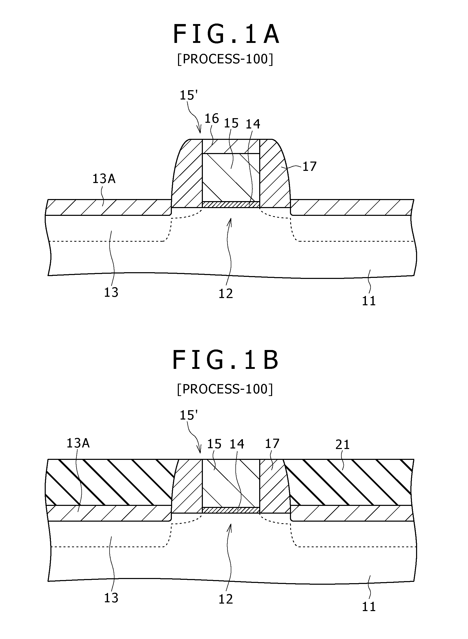
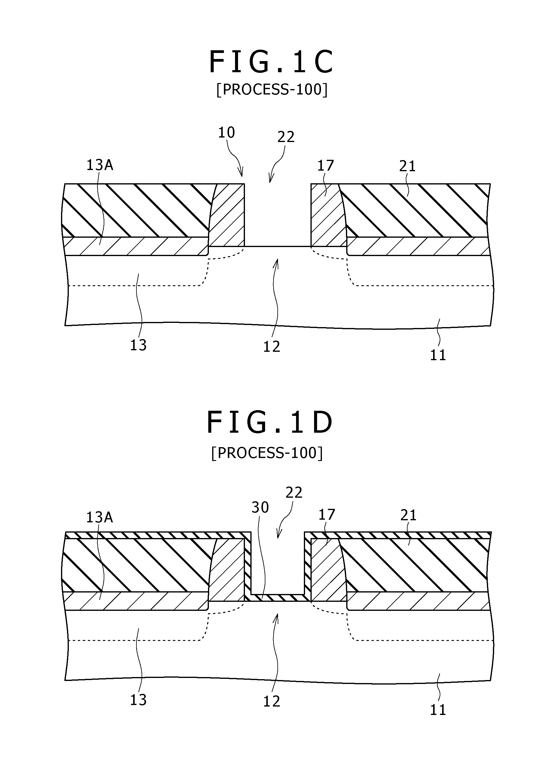
[0041]A first embodiment of the present invention relates to a method for manufacturing an insulated gate field effect transistor according to the first mode of the present invention.
[0042]As shown in the schematic partial end view of FIG. 1I, an insulated gate field effect transistor obtained by the method for manufacturing an insulated gate field effect transistor according to the first embodiment includes (A) source / drain regions 13 and a channel forming region 12, (B) a gate electrode 23 formed above the channel forming region 12, and (C) a gate insulating film 30. In the first embodiment, and in second to fourth embodiments of the present invention, which will be described later, an n-channel insulated gate field effect transistor is formed.
[0043]The gate insulating film 30 is composed of hafnium oxide. The gate electrode 23 is formed of a work function control layer 31 and a conductive material layer 32. The work function control layer 31 is composed of a conductive material (...
second embodiment
[0059]The second embodiment is a modification of the first embodiment. In the second embodiment, the insulating layer is formed of a lower insulating layer 21A and an upper insulating layer 21B formed on this lower insulating layer 21A. The lower insulating layer 21A covers at least the source / drain regions 13 (specifically, the source / drain regions 13 and the side wall film 17). In the step of removing the insulating layer, the upper insulating layer 21B is removed whereas the lower insulating layer 21A is left. The lower insulating layer 21A is composed of the same material as that of the first interlayer insulating layer 41, specifically, SiN. The upper insulating layer 21B is composed of the same material as that of the second interlayer insulating layer 42, specifically, SiOx (X=2). As the film deposition condition for the lower insulating layer 21A composed of SiN, the same condition as that shown in Table 1 can be employed. Examples of the film deposition condition for the up...
third embodiment
[0072]The third embodiment relates to a method for manufacturing an insulated gate field effect transistor according to the second mode of the present invention.
[0073]As shown in the schematic partial end view of FIG. 3B, an insulated gate field effect transistor obtained by the method for manufacturing an insulated gate field effect transistor according to the third embodiment also includes (A) source / drain regions 13 and a channel forming region 12, (B) a gate electrode 23 formed above the channel forming region 12, and (C) a gate insulating film 30.
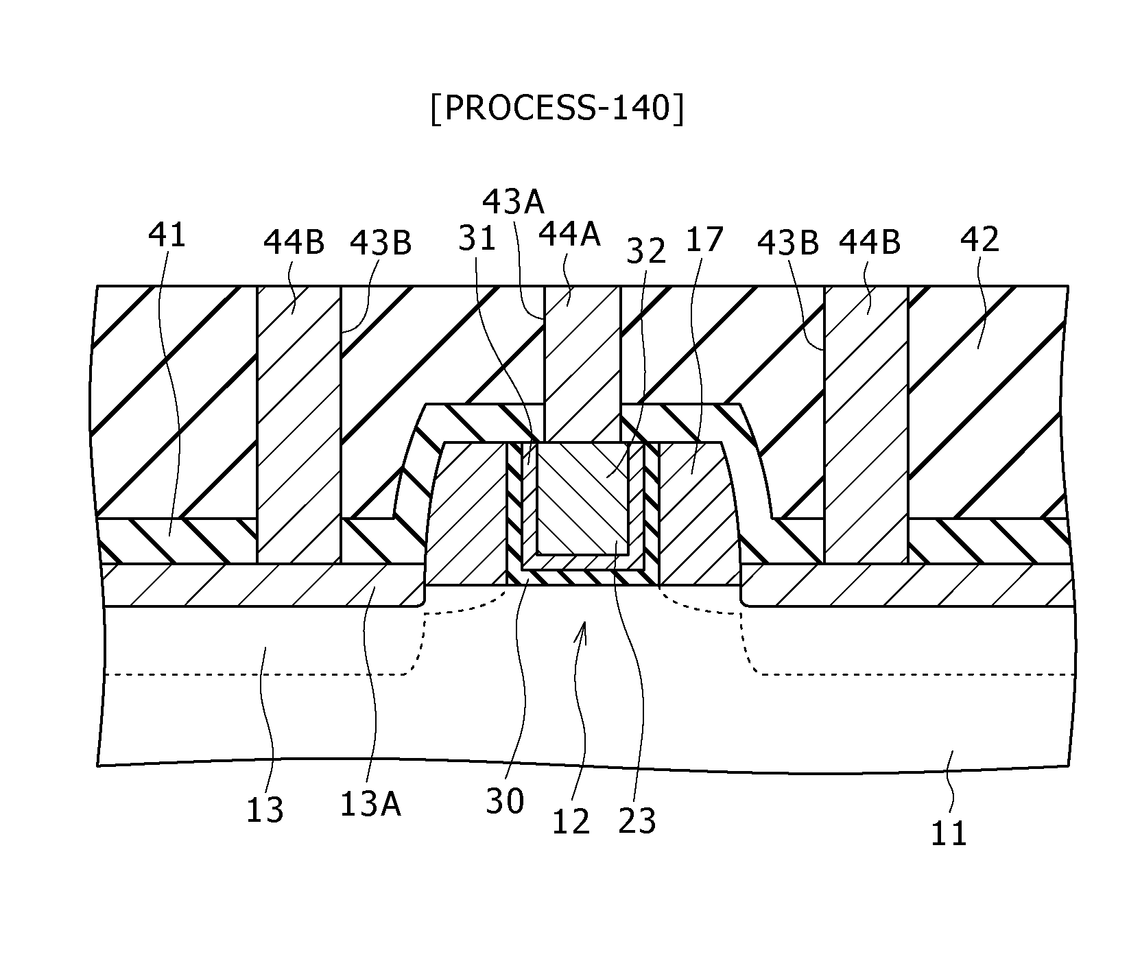
[0074]In the third embodiment, a first interlayer insulating layer 41 composed of silicon nitride (SiN) is deposited (formed) on an insulating layer 21, a side wall film 17, and the gate electrode 23, unlike the first embodiment. On the first interlayer insulating layer 41, a second interlayer insulating layer 42 composed of silicon oxide (SiOx, e.g., X=2) is deposited (formed). Furthermore, a contact plug formation opening 43A is prov...
PUM
 Abstract
Description
Claims
Application Information