Laminated and sintered ceramic circuit board, and semiconductor package including the circuit board

a technology of laminated and sintered ceramics and circuit boards, which is applied in the manufacture of printed circuits, printed circuit aspects, metallic pattern materials, etc., can solve the problems of reducing the mechanical strength of the whole semiconductor element, and fragile insulation materials with low dielectric constants, etc., to achieve sufficient rigidity, suppress thermal stress acting between the semiconductor element and the intermediate board, and high mechanical strength

Active Publication Date: 2013-07-16
NGK INSULATORS LTD
View PDF21 Cites 2 Cited by
  • Summary
  • Abstract
  • Description
  • Claims
  • Application Information

AI Technical Summary

Benefits of technology

[0042]As described above, base material of a laminated and sintered ceramic circuit board according to the present invention comprises plural dielectric layers comprising ceramic. Ceramic has a coefficient of thermal expansion close to that of silicon constituting a semiconductor element. Accordingly, even when the board joined with a semiconductor element is exposed to temperature alteration as mentioned previously, thermal stress acting between the semiconductor element and the intermediate board can be suppressed. In addition, ceramic has higher mechanical strength as compared with conventional board materials (for example, resin and the like). Accordingly, even when the thickness of the board is decreased for the purpose of making a circuit element package as mentioned previously short-in-height or the like, sufficient rigidity can be maintained. Further, in a laminated and sintered ceramic circuit board according to the present invention, an inner layer wiring comprising conductor having a complicated structure converting wiring pitch as mentioned previously is embedded within the base material. Accordingly, unlike the case as in a board according to prior art where a multilayer wiring layer consisting of material other than base material is separately formed, increase in manufacturing cost and decrease in temperature cycle reliability can be avoided.
[0043]Namely, in accordance with the present invention, a circuit board with high reliability against temperature alteration and high mechanical strength is provided. Specifically, in accordance with the present invention, a board that can decrease thermal stress acting between a semiconductor element and a board in association with temperature alteration, as well as has high mechanical strength (rigidity) as a whole board (including a multilayer wiring layer) is provided. In addition, by using such a circuit board, a fast, downsized and short-in-height (thin) semiconductor package with high reliability is provided.

Problems solved by technology

However, in general, insulating material with low dielectric constant is fragile and the strength of surface wiring tends to decrease in combination with fine-lined pitch of wirings.
In addition, the thinner a semiconductor element becomes, the lower the mechanical strength of the whole semiconductor element necessarily becomes.
Therefore, its coefficient of thermal expansion is different from that of silicon constituting a semiconductor element, and problems such as breakdown of a joining part between a semiconductor element and a package board, due to thermal stress acting between the semiconductor element and the package board in association with temperature alteration that a circuit element package suffers from, for example, on soldering the semiconductor element to the package board by means of flip-chip joining or the like, soldering the circuit element package to the circuit board by means of BGA reflow, or the like, are concerned.
However, demand for fast signal transmission, fine-lined wiring pitch and a thin element as mentioned previously goes on increasing more and more and accordingly problems such as breakdown of a joining part of a semiconductor element due to thermal stress acting on the joining part of the semiconductor element go on deepening more and more.
In addition, introduction of an intermediate board into a circuit element package leads to increase in thickness (elongation-in-height) of the circuit element package.
However, as mentioned above, since a certain level of thermal stress acts on a joining part between a semiconductor element and an intermediate board, sufficient mechanical strength (rigidity) of the intermediate board cannot be maintained when the intermediate board is made thinner for the purpose of lowering the height of a circuit element package, and consequently problems such as warpage of the intermediate board may occur due to the thermal stress acting between the semiconductor element and the intermediate board.
However, addition of such a reinforcing member may complicate the manufacturing process of a circuit element package and consequently lead to increase in the manufacturing cost of the circuit element package.
However, since, in the above-described intermediate board with base material made of silicon, glass or the like, it is difficult to configure conductor having a complicated structure like the above-mentioned inner layer within the base material, in general, a through conductor (via hole) extending in its thickness direction (direction perpendicular to its principal surfaces) is formed in the base material, and a conductor having a complicated structure converting the wiring pitch is formed within a multilayer wiring layer consisting of material other than that of the base material, which is separately formed on the semiconductor element side of the base material.
The configuration wherein a multilayer wiring layer separate from an intermediate board is disposed as described above may not only increase its manufacturing cost, but also lower its reliability (for example, temperature cycle reliability) due to detachment of the multilayer wiring layer from base material for example on repeated use or the like.
In addition, since the mechanical strength of an intermediate board with base material of, for example, silicon, glass or the like, as well as a multilayer wiring layer disposed on its principal surface is low, when the thickness thereof is decreased for the purpose of making a circuit element package as mentioned previously short-in-height, a problem that the mechanical strength of the whole intermediate board decreases may occur.

Method used


Image

  • Laminated and sintered ceramic circuit board, and semiconductor package including the circuit board
  • Laminated and sintered ceramic circuit board, and semiconductor package including the circuit board
  • Laminated and sintered ceramic circuit board, and semiconductor package including the circuit board

Examples


example

1. Configuration of Laminated and Sintered Ceramic Circuit Board According to Embodiment of the Invention

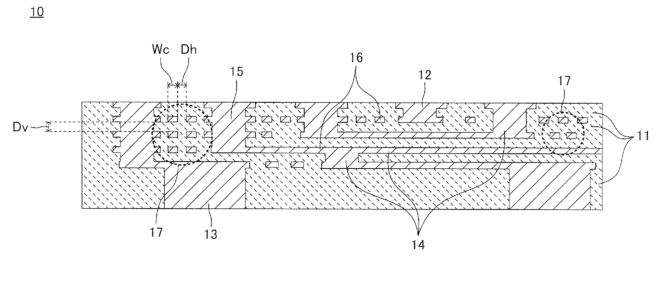
[0153]As mentioned previously, FIG. 1 is a schematic longitudinal sectional view of a laminated and sintered ceramic circuit board according to one embodiment of the present invention. More specifically, FIG. 1 is a schematic view of cross section surface by a plane perpendicular to the principal surfaces (longitudinal section surface) of the laminated and sintered ceramic circuit board according to one embodiment of the present invention. As shown in FIG. 1, the laminated and sintered ceramic circuit board 10 according to one embodiment of the present invention comprises base material 11 that comprises plural dielectric layers comprising ceramic, one or more first surface electrodes 12 disposed to expose at a first principal surface that is one surface of two principal surfaces of the board 10 and comprising conductor, one or more second surface electrodes 13 disposed to expose ...


PUM


Abstract

A circuit board that can decrease thermal stress acting between a semiconductor element and a board in association with temperature alteration and has high mechanical strength (rigidity) as a whole board (including a multilayer wiring layer) is provided. Ceramic base material having a coefficient of thermal expansion close to that of a semiconductor element and inner layer wiring are integrally sintered, and the circuit board is configured so that fine-lined conductor structure corresponding to a multilayer wiring layer in the inner layer wiring has predetermined width, intralayer interval and interlayer interval. Thereby, thermal stress acting between a semiconductor element and the board when the board is exposed to temperature alteration in a condition where it is joined with the semiconductor element is suppressed, rigidity of the board is maintained, and its reliability against temperature cycle is increased.

Description

BACKGROUND OF THE INVENTION[0001]1. Field of the Invention[0002]The present invention relates to a laminated and sintered ceramic circuit board. Specifically, the present invention relates to a laminated and sintered ceramic circuit board having a fine-lined inner layer wiring. Further, the present invention also relates to a semiconductor package including the laminated and sintered ceramic circuit board.[0003]2. Description of the Related Art[0004]Responding to rising performance and downsizing of electronic devices and the like, market need to fast, downsized and short-in-height (thin) circuit element packages used in various electronic devices (for example, semiconductor packages such as IC packages and the like) have been going on increasing. As a result, in a circuit element (for example, a semiconductor element such as an IC chip, a resistive element, a capacitative element, an inductor element and the like) constituting a circuit element package, especially in a semiconducto...

Claims


Application Information

Patent Timeline
Patent Type & Authority Patents(United States)
IPC IPC(8): H01L23/48H01L23/40H01L23/52
CPCH01L23/49822H01L23/15H01L23/49827H05K3/4629H05K2201/0191H05K2201/068H01L2924/0002H05K2201/09227H05K2201/09236H05K2201/09672H01L2924/00
Inventor TANI, MAKOTOHIRAI, TAKAMIYANO, SHINSUKENANATAKI, TSUTOMU
Owner NGK INSULATORS LTD
Why Eureka
Try Eureka