Heat-resistant adhesive sheet for semiconductor device fabrication, adhesive used for the sheet, and method for fabricating semiconductor device using the sheet

a technology of heat-resistant adhesive and semiconductor devices, which is applied in the direction of film/foil adhesives, basic electric elements, transportation and packaging, etc., can solve the problems of difficult peeling off of heat-resistant adhesive sheets, the method is not intended for substrateless semiconductor devices, and the subsequent electrode formation step is not smooth, so as to improve the fabrication yield of semiconductor packages

Inactive Publication Date: 2013-08-06
NITTO DENKO CORP
View PDF6 Cites 3 Cited by
  • Summary
  • Abstract
  • Description
  • Claims
  • Application Information

AI Technical Summary

Benefits of technology

[0028]Alternatively, the epoxy resin component may have a weight per epoxy equivalent of less than or equal to 1000 g / eq, the adhesive layer may contain a conductive filler to impart electrical conductivity and high elasticity to the adhesive layer.
[0030]The present invention provides an adhesive sheet for temporarily fixing chips, used in a method for fabricating a substrateless semiconductor package that does not use a metal lead frame (for example a method for fabricating WLP), an adhesive used in the adhesive sheet, and a method for fabricating a semiconductor device using the adhesive sheet. The adhesive of the present invention contains an appropriate content of a rubber component to add flexibility to the adhesive sheet without impairing heat resistance of the adhesive sheet. Accordingly, the adhesive sheet exhibits good machinability in cutting of the adhesive sheet.
[0032]The present invention can improve the fabrication yield of the semiconductor packages.

Problems solved by technology

Furthermore, since the chips need to be unfixed after the chips have been encapsulated with resin and formed into individual packages, the supporter need to be removable, instead of permanent bonding fixation.
Obviously, the method is not intended for substrateless semiconductor devices and the adhesive layer is chosen by taking into consideration the adhesiveness to a substrate.
The following problems can arise with the following method for fabricating a substrateless semiconductor package using an adhesive tape as a temporary supporter.
Consequently, the positions of chips encapsulated in the packages resulting from dicing would vary from one package to another and a subsequent electrode formation step would not smoothly be performed and partially encapsulated packages would result.
Therefore it can be difficult to peel off the heat-resistant adhesive sheet 2 for semiconductor device fabrication, or adhesive deposits 9 as illustrated in FIG. 3 can occur or static electricity can build up during peeling.
As peeling becomes difficult, more time is required accordingly.
Heavy peeling therefore can lead to reduction in productivity.
Static electricity build-up caused by peeling leads to a problem due to adhesion of dust in a subsequent step.
When the heat-resistant adhesive sheet 2 for semiconductor device fabrication is peeled off, packages can be damaged by adhesion strength to the chips increased by curing of the encapsulation material or heat.
Furthermore, if gas is generated from the adhesive layer or part of the adhesive is eluted from the adhesive layer under heat generated during use of the device, the gas or adhesive can contaminate the surfaces of the chips and subsequent steps such as the electrode formation step cannot reliably be performed, thus resulting in poor connections.

Method used


Image

  • Heat-resistant adhesive sheet for semiconductor device fabrication, adhesive used for the sheet, and method for fabricating semiconductor device using the sheet
  • Heat-resistant adhesive sheet for semiconductor device fabrication, adhesive used for the sheet, and method for fabricating semiconductor device using the sheet
  • Heat-resistant adhesive sheet for semiconductor device fabrication, adhesive used for the sheet, and method for fabricating semiconductor device using the sheet

Examples


working examples

[0076]A measuring method used in working examples is as follows.

[0077]Initial adhesion strength to SUS: Peel adhesion strength to a SUS304BA plate at an angle of 180° at room temperature

[0078]Peel strength from package: Peel adhesion strength at an angle of 180° when the adhesive tape is peeled from the package

[0079]Chip displacement: Displacement from the initial position of a chip measured with a digital microscope after package fabrication

[0080]Adhesive deposit: The surface of the package was visually checked for adhesive deposits after the adhesive tape was peeled off.

[0081]The present invention will be descried more specifically with respect to working examples. The term “part” in the following description means “part by weight”.

working example 1

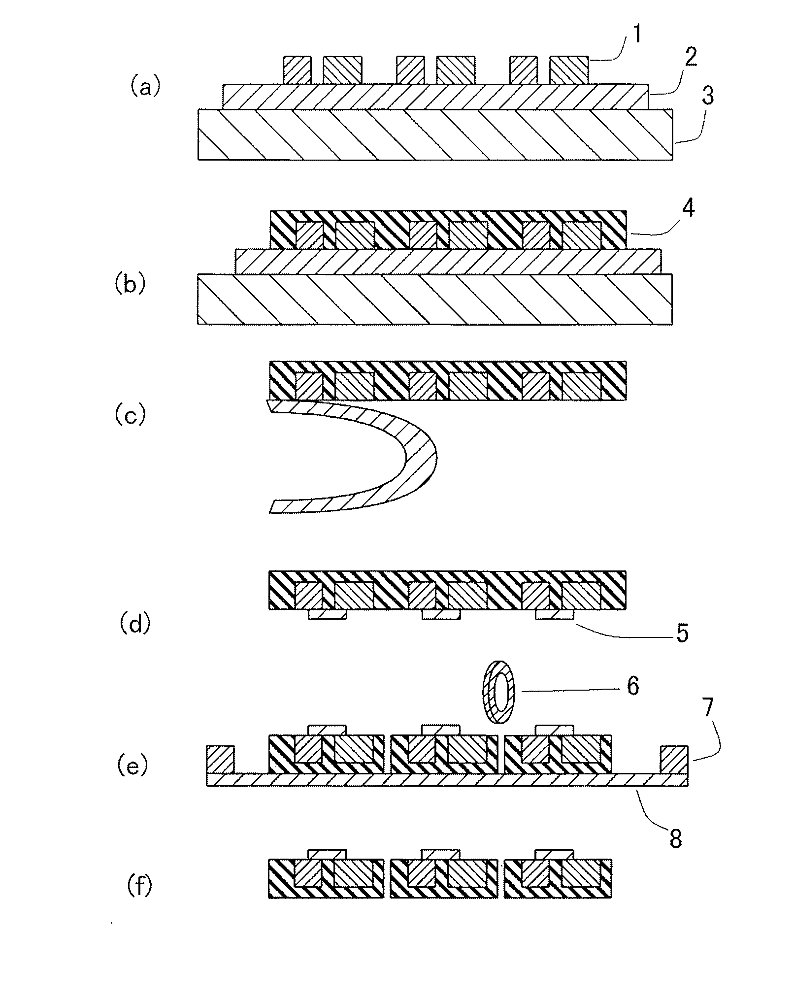
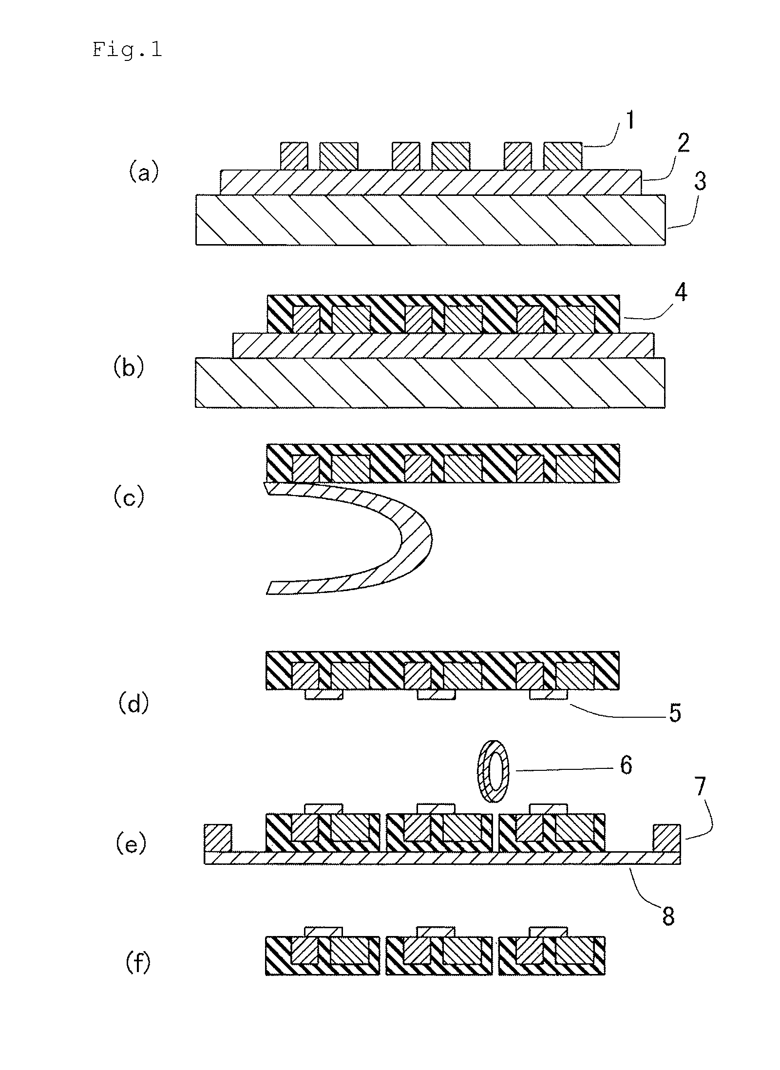
[0082]42 parts of acrylonitrile-butadiene rubber (Nipol 1072) from Zeon Corporation), 53 parts of bisphenol A-type epoxy resin (Epikote 828 from Japan Epoxy Resin Co., Ltd., with a weight per epoxy equivalent of 190 g / eq), and 5 parts of imidazole (C1 1Z from Shikoku Chemicals Corporation) were blended and dissolved in an MEK solvent to a concentration of 35 wt % to prepare a bond solution. The bond solution was applied to a 35-μm-thick copper foil serving as a base material film, and was then dried at 150° C. for 3 minutes to form an adhesive layer having a thickness of 10 μm, thus forming a heat-resistant adhesive sheet for semiconductor device fabrication.

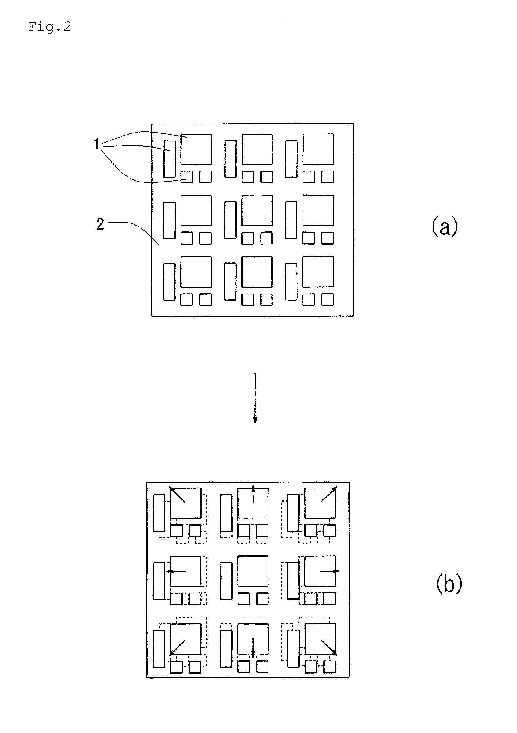
[0083]A 3 mm×3 mm Si wafer chip was placed on the heat-resistant adhesive tape, epoxy-based encapsulation resin powder (GE-740LA from Nitto Denko Corporation) was sprinkled over the tape and the wafer chip, and then molded by heating at a temperature of 175° C. under a pressure of 3.0 kg / cm2 for 2 minutes. Then the structure was...

working example 2

[0084]24 parts of acrylonitrile-butadiene rubber (Nipol 1072) from Zeon Corporation), 65 parts of bisphenol A-type epoxy resin (Epikote 1002 from Japan Epoxy Resin Co., Ltd., with a weight per epoxy equivalent of 650 g / eq), 10 parts of phenol resin (P-180 from Arakawa Chemical Industries, Ltd.), and 1 part of triphenylphosphane (TPP from Hokko Chemical Industry) were blended and dissolved in an MEK solvent to a concentration of 35 wt % to prepare an adhesive solution. The adhesive solution was applied to a 35-μm-thick copper foil serving as the base material film, and was then dried at 150° C. for 3 minutes to form an adhesive layer having an adhesive thickness of 10 μm, thus forming a heat-resistant adhesive sheet for semiconductor device fabrication. The rest of the method for fabricating the package was the same as that in Working Example 1.


PUM

PropertyMeasurementUnit
temperaturesaaaaaaaaaa
temperatureaaaaaaaaaa
glass transition temperatureaaaaaaaaaa

Abstract

The present invention provides a heat-resistant adhesive sheet for semiconductor device fabrication that is attached to a substrateless semiconductor chip when the chip is encapsulated with resin. The adhesive sheet includes a base material layer and an adhesive layer. The adhesive layer contains a rubber component and an epoxy resin component. The proportion of the rubber component in an organic substance in the adhesive is in the range of 20 to 60 wt %.

Description

CROSS REFERENCE TO RELATED APPLICATIONS[0001]The disclosure of Japanese Patent Application No. 2009-285570 filed on Dec. 16, 2009 including the specification, drawings and abstract is incorporated herein by reference in its entirely.BACKGROUND OF THE INVENTION[0002]1. Field of the Invention[0003]The present invention relates to a heat-resistant adhesive sheet for semiconductor device fabrication used for fabrication of substrateless semiconductor packages that do not use a metal lead frame, an adhesive used for the sheet, and a method for fabricating a semiconductor device using the sheet.[0004]2. Description of the Related Art[0005]Among LSI packaging technologies, Chip Size / Scale Package (CSP) technologies have recently come into attention. Among those technologies, a package form that does not use a substrate and packs only chips, such as Wafer Level Package (WLP), is especially attractive in terms of packaging density and size reduction. In a WLP fabrication method, multiple sem...

Claims


Application Information

Patent Timeline
Patent Type & Authority Patents(United States)
IPC IPC(8): H01L23/28C09J7/20
CPCC09J7/02H01L21/568H01L24/24H01L24/96Y10T428/287C09J2421/00C09J2463/00H01L23/3107H01L23/3114H01L23/5389H01L2224/24137H01L2924/01013H01L2924/01029H01L2924/01032H01L2924/01033H01L2924/01047H01L2924/01051H01L2924/01079H01L2924/01082C09J2203/326H01L2924/01078H01L2924/01005H01L2924/01006H01L2924/01019H01L2924/01024H01L2924/01042H01L2924/01075H01L2924/181C09J7/20H01L2924/00
Inventor YANAGI, YUICHIROKIUCHI, KAZUYUKIHOSHINO, SHINJI
Owner NITTO DENKO CORP
Why Eureka
Try Eureka