Heat sink and its manufacturing method

a technology of heat sink and manufacturing method, which is applied in the direction of solid-state devices, basic electric elements, lighting and heating apparatus, etc., can solve the problems of only meeting the limit of cooling with the use of heat sinks based on these materials, the heat radiation characteristics of heat sinks are not always satisfactory, and the amount of heat emitted from each electronic component is larg

Inactive Publication Date: 2004-07-06
TOKUYAMA CORP
View PDF12 Cites 7 Cited by
  • Summary
  • Abstract
  • Description
  • Claims
  • Application Information

AI Technical Summary

Benefits of technology

The present inventor has found that a polycrystalline diamond film of high quality exhibiting high thermal conductivity can be produced on a ceramic substrate containing aluminum nitride as a principal component by preliminarily forming thereon a layer of specified substance exhibiting excellent adhesion to the substrate and a diamond film and thereafter forming a polycrystalline diamond film on the above layer in accordance with the vapor phase method.
In the above heat sink of the present invention, a ceramic substrate containing, as a principal component, aluminum nitride which is excellent in insulating characteristics and heat radiation characteristics is used as a substrate material. Accordingly, the heat absorption performance and heat radiation performance of the heat sink as a whole are excellent. Further, in case of the heat sink having such a structure that the diamond film is formed so as not to cover the entire surface of the substrate, an electronic circuit made of a metal can be printed on the substrate without the particular need to form an insulating film.
In the heat sink of the present invention, it is preferred that the bonding member be constituted of at least one material selected from the group consisting of silicon, silicon carbide, tungsten, tungsten carbide, CuW, Cu--Mo alloy, Cu--Mo--W alloy, amorphous carbon, boron nitride, carbon nitride and titanium. In the use of this bonding member, cracking or other faults of the diamond film superimposed on the bonding member can be avoided, the heat radiation performance is enhanced, and the durability of the diamond film is prolonged.
According to necessity, the polycrystalline silicon may contain a dopant. The addition of the dopant would enable enhancing the orientation of polycrystalline silicon and would also enable imparting electrical conductivity to the silicon film.
In the heat sink of the present invention, preferably, the diamond film layer exhibits a thermal conductivity of 800 W / mK or greater. The heat sink of the present invention attains enhanced thermal conductivity as compared with that of a heat sink wherein a diamond film layer is directly superimposed on a substrate.
In the above process of the present invention, peeling or cracking of the diamond film would not occur during the cooling step after the diamond film formation step wherein the substrate is maintained at 700 to 1100.degree. C. Thus, a heat sink of high quality according to the present invention can be stably produced in high efficiency in the process of the present invention. In particular, when a layer of crystalline substance orientated for a specified crystal face is formed as the bonding member layer, a diamond film of large crystal grains and high crystallinity can be easily formed. Moreover, when a layer containing silicon as a principal component is formed as the bonding member layer, a diamond nucleation would be promoted, thereby enabling formation of a diamond film in higher efficiency. Furthermore, in the process wherein the bonding member layer is formed from a conductive substance, such as a polycrystalline silicon containing a dopant, and wherein, while a direct current voltage is applied to the bonding member layer, a thin diamond film is formed on the bonding member layer in accordance with microwave CVD or hot filament CVD method, it would be feasible to efficiently deposit an effective precursor for diamond film synthesis on the substrate surface, thereby easily forming a diamond film of high crystallinity, high orientation degree and high thermal conductivity.

Problems solved by technology

Thus, currently a large amount of heat is emitted from each electronic component.
However, as a result of integration of electronic components, the outgoing heat is increasing to such an extent that the cooling with the use of a heat sink based on these materials only encounters a limit.
However, the heat radiation characteristics of this heat sink have not always been satisfactory because the single crystal diamond is so expensive that a heat sink of large configuration cannot be employed and because the brazing material becomes a resistor to heat conduction.
However, this insulating film often poses a problem with respect to the reliability in voltage withstanding properties, etc.
However, it is difficult to directly form a polycrystalline diamond layer of high quality on a substrate of sintered aluminum nitride (AlN) in accordance with the vapor phase synthetic process.
In this connection, the diamond film is so thin that the thermal conductivity thereof cannot be directly measured.
On the other hand, when the substrate temperature exceeds 1200.degree. C., the bonding member layer may suffer damages.
Therefore, the substrate temperature exceeding 1200.degree. C. is unfavorable.
However, these conditions depend on the capacity and morphology of apparatus used in the above synthesis and should not be determined generally.

Method used


Image

  • Heat sink and its manufacturing method
  • Heat sink and its manufacturing method
  • Heat sink and its manufacturing method

Examples


example 1

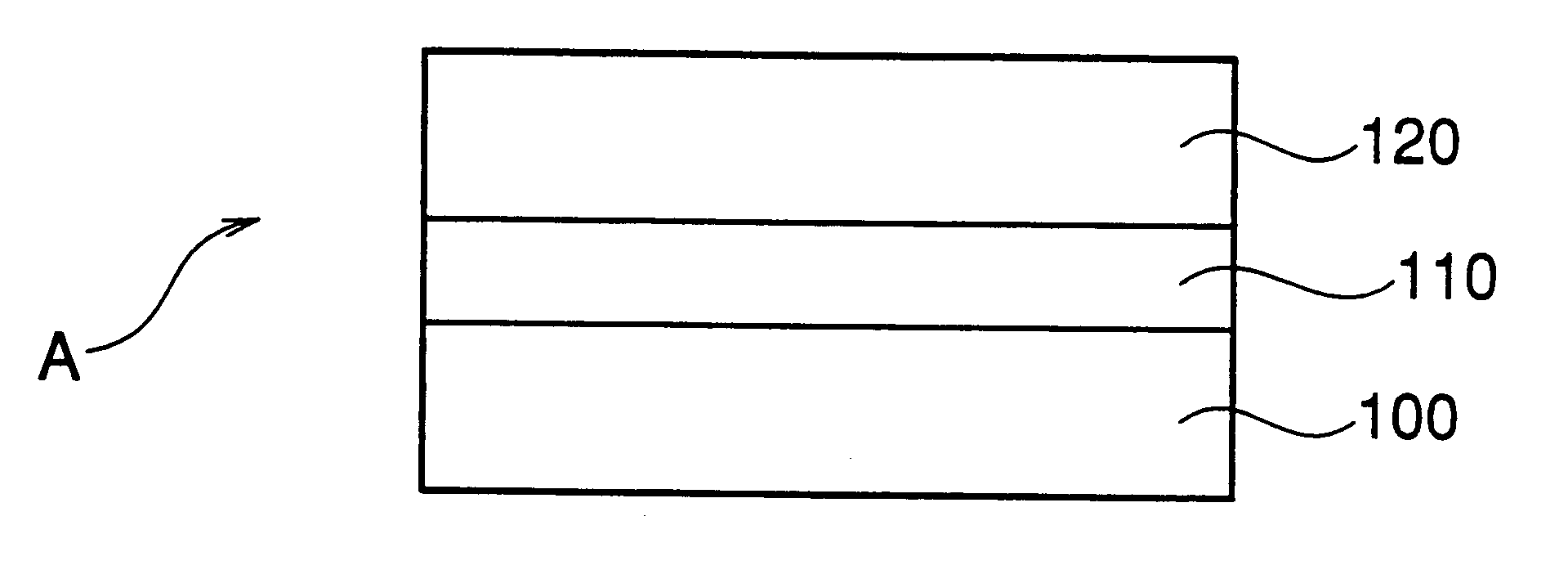
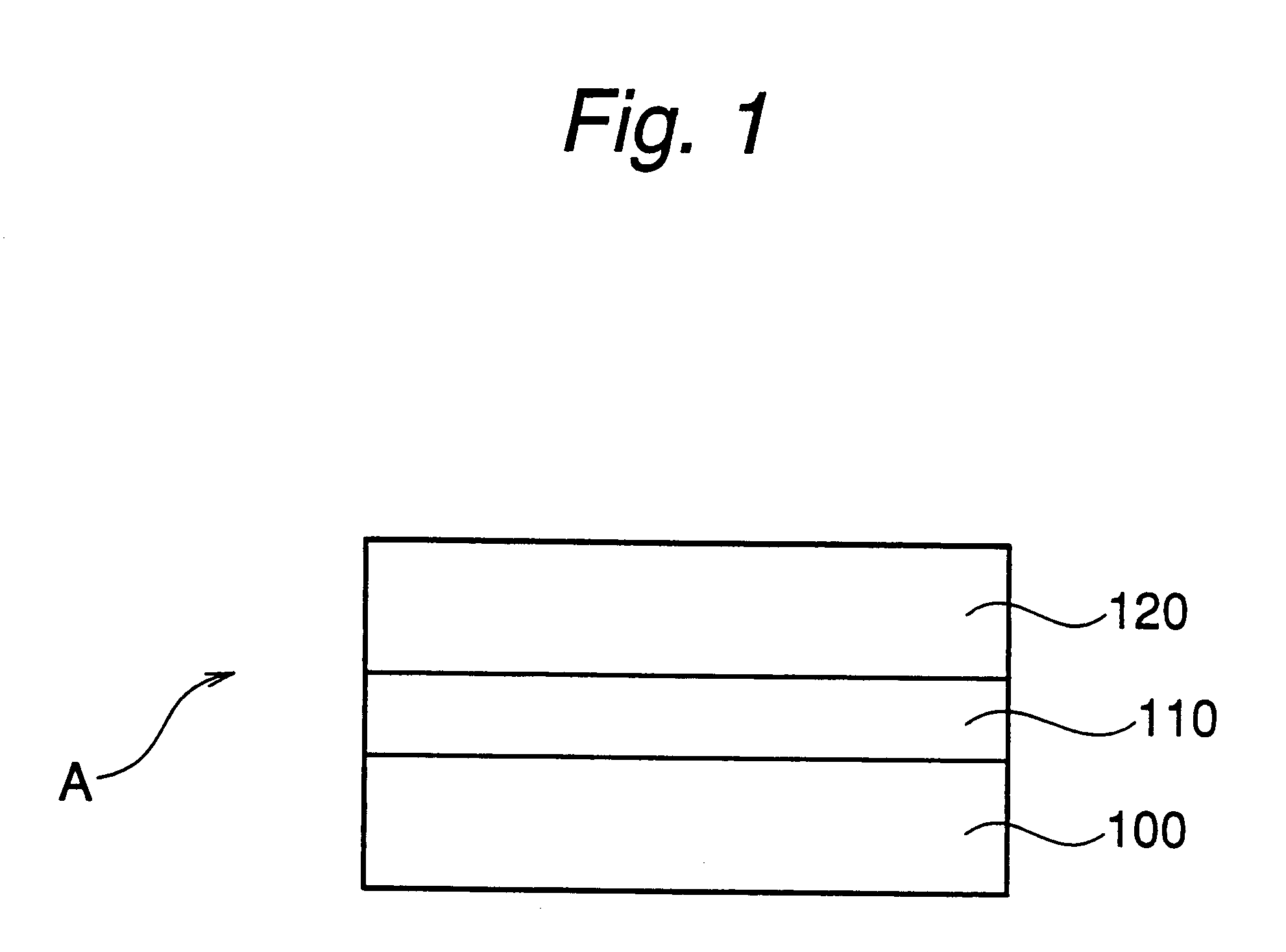
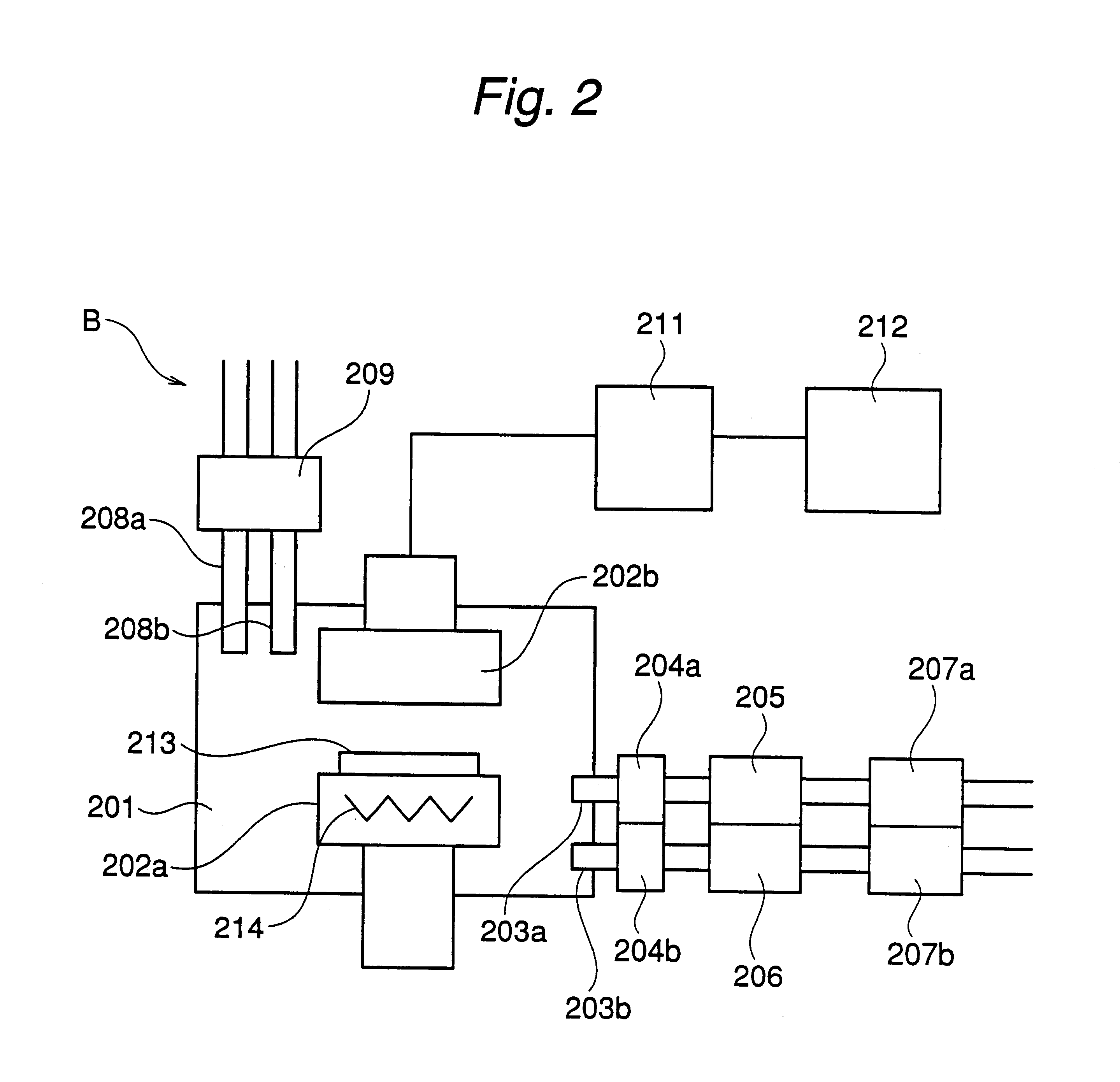
Ceramic substrate (25 mm.times.25 mm.times.0.5 mm thickness) containing aluminum nitride as a principal component was set on the substrate mounting table inside the radio frequency plasma CVD apparatus. The interior of the reaction vessel was exhausted to vacuum, and simultaneously the substrate mounting table was heated to 120.degree. C. The apparatus was held undisturbed for about 30 min until the substrate temperature was stabilized, and the reduction of pressure within the reaction vessel to 5.times.10.sup.-6 Torr or below was confirmed. Monosilane gas and hydrogen were introduced in the reaction vessel at respective flow rates of 3 cc / min and 100 cc / min, and the internal pressure of the reaction vessel was set for 1.5 Torr by regulating the exhaust valve. Subsequently, radiofrequency wave from the radiofrequency power source at an output of 50 W was tuned by the tuner so as to minimize reflection loss and inputted to the radiofrequency application electrode. Radiofrequency powe...

example 2

Heat sink was produced in the same manner as in Example 1 except that the thickness of synthesized diamond film was 200 .mu.m. The diamond film on the substrate was visually inspected, and it was found that formation of the diamond film extended to edges of the substrate and that there was no film peeling. A section of the diamond film was observed through a microscope, and the thickness of the diamond film was measured. It was found that the thickness was about 200 .mu.m. Thereafter, the crystallinity of the diamond on the substrate was inspected in the same manner as in Example 1. As a result, it was found that the FWHM was about 6.8 cm.sup.-1. Further, the orientation of the obtained diamond layer was inspected, and no result of strong orientation on a specified face was recognized. Still further, the thermal conductivity of the obtained heat sink was measured. The measurement showed that the thermal conductivity after lamination with the diamond film was about 720 W / mK while tha...

example 3

Heat sink was produced in the same manner as in Example 1 except that the bonding member layer was constituted of W. The diamond film on the substrate was visually inspected, and it was found that formation of the diamond film extended to edges of the substrate and that there was no film peeling. A section of the diamond film was observed through a microscope, and the thickness of the diamond film was measured. It was found that the thickness was about 50 .mu.m. Thereafter, the crystallinity of the diamond on the substrate was inspected. As a result, it was found that the FWHM was about 8.0 cm.sup.-1. Further, the orientation of the obtained diamond layer was inspected, and no result of strong orientation on a specified face was recognized. Still further, the thermal conductivity of the obtained heat sink was measured. The measurement showed that-the thermal conductivity after lamination with the diamond film was about 360 W / mK while that after lamination with the bonding member lay...


PUM

PropertyMeasurementUnit
thicknessaaaaaaaaaa
thermal conductivityaaaaaaaaaa
thicknessaaaaaaaaaa

Abstract

A heat sink including a substrate of insulating ceramic and, superimposed on its upper surface, a diamond film for disposing an element thereon. The heat sink has excellent heat radiation characteristics and is stable during use. This heat sink is obtained by providing a substrate of ceramic containing aluminum nitride of high thermal conductivity as a principal component; forming on the substrate a bonding member layer, such as a silicon film which is capable of being bonded with the substrate and a diamond film; and forming a polycrystalline diamond film of high quality on the bonding member layer so that the polycrystalline diamond film is strongly bonded with the substrate via the bonding member layer interposed therebetween in accordance with, for example, the vapor phase method.

Description

1. Technical FieldThe present invention relates to a heat sink and a process for producing the same. More particularly, the present invention relates to a heat sink having such a laminate structure that a layer of diamond of high thermal conductivity is superimposed on a substrate of aluminum nitride of high thermal conductivity, and further relates to a process for producing the heat sink.2. Description of the Prior ArtThe processing capacity of electronic components is making striking enhancement in accordance with the increase of information density. Thus, currently a large amount of heat is emitted from each electronic component. Since maintaining constant temperature is desired for ensuring the stable functioning of electronic components, various improvements for cooling them have been proposed. It is common practice to, in practical use, mount electronic components tending to have high temperature on a heat radiating member, namely, a material capable of absorbing heat, or a d...

Claims


Application Information

Patent Timeline
Patent Type & Authority Patents(United States)
IPC IPC(8): H01L21/02H01L23/373H01L21/48H01L23/34C04B37/00C04B41/87C04B41/89C04B41/90
CPCH01L21/4882H01L23/3731H01L23/3732H01L23/3735Y10T29/4935H01L2924/0002H01L2924/00
Inventor AZUMA, MASANOBU
Owner TOKUYAMA CORP
Why Eureka
Try Eureka