
Roll-to-roll non-vacuum deposition of transparent conductive electrodes

a technology of transparent conductive electrodes and conductive electrodes, which is applied in the direction of basic electric elements, electrical equipment, semiconductor devices, etc., can solve the problems of poor surface coverage, low vacuum deposition process equipment, and non-uniform three-dimensional distribution of elements, so as to reduce or eliminate the amount of material, the effect of low cos

Inactive Publication Date: 2013-09-10
AERIS CAPITAL SUSTAINABLE IP
View PDF64 Cites 10 Cited by
  • Summary
  • Abstract
  • Description
  • Claims
  • Application Information

AI Technical Summary

Benefits of technology

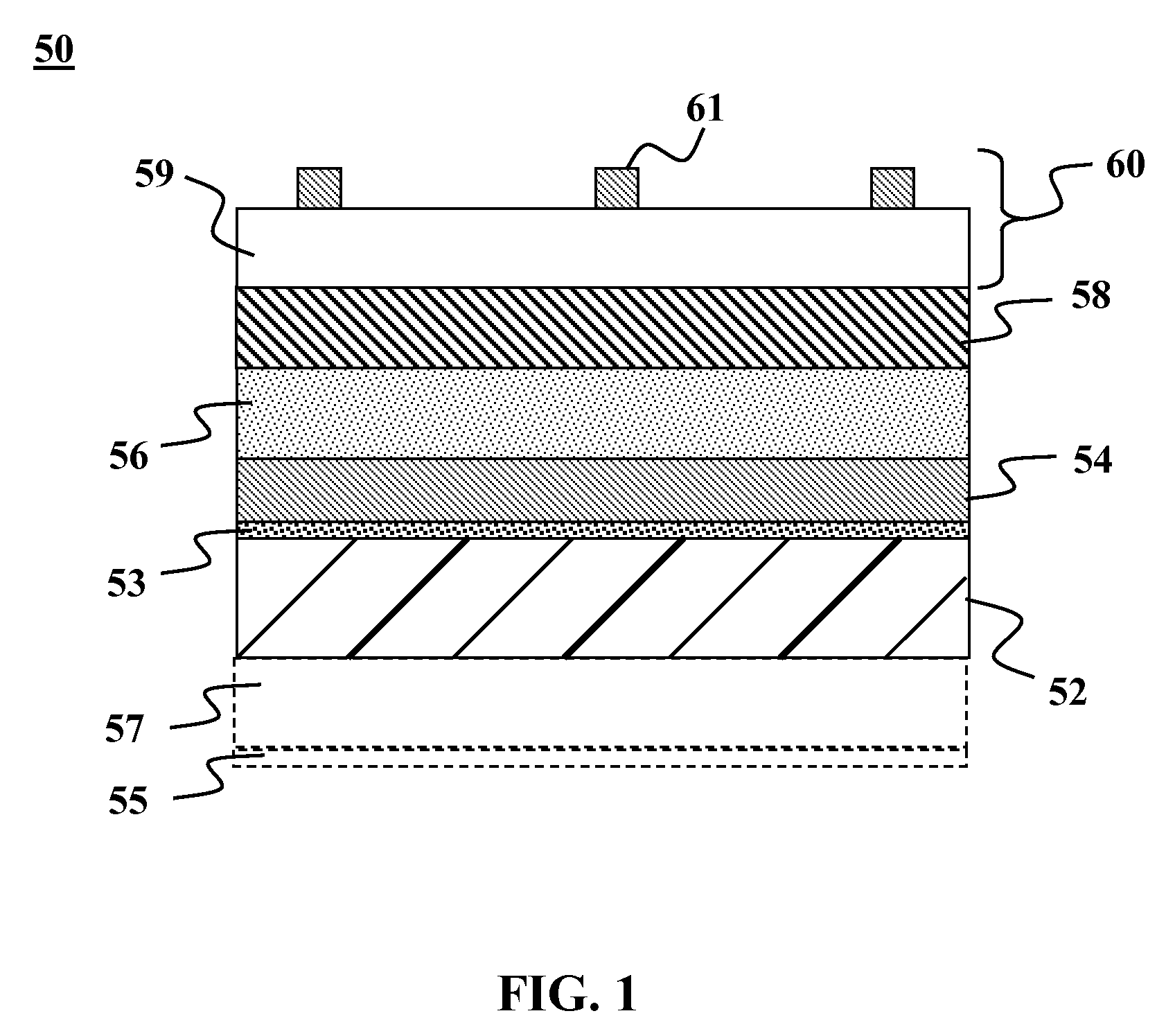
[0012]Embodiments of the present invention address at least some of the drawbacks set forth above. It should be understood that at least some embodiments of the present invention may be applicable to any type of solar cell, whether they are rigid or flexible in nature or the type of material used in the absorber layer. Embodiments of the present invention may be adaptable for roll-to-roll and / or batch manufacturing processes. In one embodiment, low cost transparent conductor (TC) is provided that will work on printed & rapid thermally processed CIGS, CIGSS, or other absorber layer to reduce or eliminate the amount of material that needs to be sputtered or chemical vapor deposited. At least some of these and other objectives described herein will be met by various embodiments of the present invention.
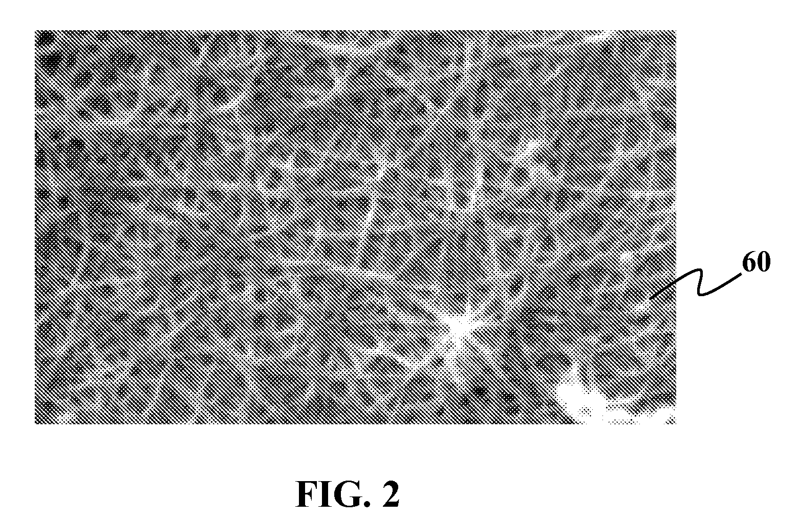
[0018]In one embodiment of the present invention, the transparent electrode of a solar cell is replaced in part by a carbon nanotubes coating that is less than one monolayer of tubes. In this embodiment, to address any roughness of underlying CIGS / ZnO(i), thicker insulator (either i-ZnO or other material) may be used. One can imagine that the ZnO(i) would not be able to completely cover the rough CIGS or CIGSS surface and that these tubes can find their way anywhere and seem to be a continuous network of highly conducting wires. The evaporation of Ni,Al fingers will go into the CIGS layer and create a shunt since the tube network is porous and the ZnO(i) is presumably spotty. Using a thicker insulator or one of the other solutions described herein will reduce shunting in rough absorber layers using web-like transparent conductors.
[0019]In another embodiment of the present invention, the method comprises processing a precursor layer in one or more steps to form a photovoltaic absorber layer; depositing a smoothing layer to fill gaps and depression in the absorber layer to reduce a roughness of the absorber layer; adding an insulating layer over the smoothing layer; and forming a web-like layer of conductive material over the insulating layer.
[0020]In yet another embodiment of the present invention, a method comprises processing a precursor layer in one or more steps to form a photovoltaic absorber layer; and depositing a smoothing, insulating layer to fill gaps and depression in the absorber layer to reduce a roughness of the absorber layer.
[0021]It should be understood that for any of the embodiments herein, the following may optionally also apply. Optionally, the smoothing insulator is sufficient to cover all peaks of the rough absorber, but sufficiently thin to allow electrons to pass out of the absorber layer. Optionally, the smoothing insulator conformally covers all peaks in the rough absorber. Optionally, the method includes further comprising creating the absorber layer by processing the precursor layer into a solid film and then thermally reacting the solid film in an atmosphere containing at least an element of Group VIA of the Periodic Table to form the photovoltaic absorber layer. Optionally, creating the absorber layer by thermal reaction of the precursor layer in an atmosphere containing at least an element of Group VIA of the Periodic Table to form the photovoltaic absorber layer. Optionally, Group IB and / or IIIA hydroxide comprises indium-gallium hydroxide and used as a precursor material for the absorber layer. Optionally, the web material may be solution coated onto the target surface. Examples of solution deposition methods may include at least one method from the group comprising: wet coating, spray coating, spin coating, doctor blade coating, contact printing, top feed reverse printing, bottom feed reverse printing, nozzle feed reverse printing, gravure printing, microgravure printing, reverse microgravure printing, comma direct printing, roller coating, slot die coating, meyerbar coating, lip direct coating, dual lip direct coating, capillary coating, ink-jet printing, jet deposition, spray deposition, aerosol spray deposition, dip coating, web coating, microgravure web coating, or combinations thereof. These applications of carbon nanotubes provide new avenues to lower costs, better durability, better thermal stability, and higher efficiencies. Of course, other non-solution based techniques may also be used.
[0022]In yet another embodiment of the present invention, a method is provided comprising of processing a precursor layer in one or more steps to form a photovoltaic absorber layer; and depositing a conformal insulating layer over the gaps and depression in the absorber layer to minimize shunting due to roughness of the absorber layer.

Problems solved by technology

These electronic devices have been traditionally fabricated using silicon (Si) as a light-absorbing, semiconducting material in a relatively expensive production process.
A central challenge in cost-effectively constructing a large-area CIGS-based solar cell or module involves reducing processing costs and material costs.
The nature of vacuum deposition processes requires equipment that is generally low throughput and expensive.
Vacuum deposition processes are also typically carried out at high temperatures and for extended times. Traditional sputtering or co-evaporation techniques are limited to line-of-sight and limited-area sources, tending to result in poor surface coverage and non-uniform three-dimensional distribution of the elements.
Unfortunately, for the film thickness and high vacuum required, sputter deposition is a slow process with an undesired low throughput / capex ratio.
In addition, material yield is low due to deposition of material onto the chamber walls.
Furthermore, temperature control during sputter deposition can limit the throughput even further, especially when damage of underlying temperature-sensitive layers, like e.g. the CIGSe / CdS stack, needs to be prevented.
Finally, controlling the large-area uniformity of both the conductivity and transparency of a sputter-deposited TCO is challenging.
A huge disadvantage of this method is the temperature required to get dense layers.
Temperatures required to sinter these layers damage the underlying films as used in thin-film PV.
One big disadvantage of this approach is the limited lateral electrical conductivity that can be accomplished without loosing too much optical transparency.
The two-phase nature of this approach limits the contact area that can be achieved at both interfaces when sandwiched between other (semi)conductive layers.
This limited contact area affects the contact resistance in a negative way.
Additionally, a possible mismatch in the coefficients of thermal expansion of both the conductive and insulating materials might impact the temperature dependence and reliability of the overall conductivity of the bi-continuous network in a negative way.

Method used


Image

  • Roll-to-roll non-vacuum deposition of transparent conductive electrodes
  • Roll-to-roll non-vacuum deposition of transparent conductive electrodes
  • Roll-to-roll non-vacuum deposition of transparent conductive electrodes

Examples


Embodiment Construction

[0029]It is to be understood that both the foregoing general description and the following detailed description are exemplary and explanatory only and are not restrictive of the invention, as claimed. It may be noted that, as used in the specification and the appended claims, the singular forms “a”, “an” and “the” include plural referents unless the context clearly dictates otherwise. Thus, for example, reference to “a material” may include mixtures of materials, reference to “a compound” may include multiple compounds, and the like. References cited herein are hereby incorporated by reference in their entirety, except to the extent that they conflict with teachings explicitly set forth in this specification.

[0030]In this specification and in the claims which follow, reference will be made to a number of terms which shall be defined to have the following meanings:

[0031]“Optional” or “optionally” means that the subsequently described circumstance may or may not occur, so that the des...


PUM

PropertyMeasurementUnit
thicknessaaaaaaaaaa
thicknessaaaaaaaaaa
thicknessaaaaaaaaaa

Abstract

Methods and devices are provided for improved photovoltaic devices. Non-vacuum deposition of transparent conductive electrodes in a roll-to-roll manufacturing environment is disclosed. In one embodiment, a method is provided for forming a photovoltaic device. The method comprises processing a precursor layer in one or more steps to form a photovoltaic absorber layer; depositing a smoothing layer to fill gaps and depression in the absorber layer to reduce a roughness of the absorber layer; adding an insulating layer over the smooth layer; and forming a web-like layer of conductive material over the insulating layer. By way of nonlimiting example, the web-like layer of conductive material comprises a plurality of carbon nanotubes. In some embodiments, the absorber layer is a group IB-IIIA-VIA absorber layer.

Description

CROSS-REFERENCE TO RELATED APPLICATION[0001]The present application claims the benefit of priority to U.S. Provisional Patent Application Ser. No. 61032425 filed Feb. 28, 2008 and fully incorporated herein by reference for all purposes.FIELD OF THE INVENTION[0002]The present invention is directed to non-vacuum depositing transparent conductive electrodes (TCE) on large area substrates and more specifically to non-vacuum TCE deposition in high-throughput roll-to-roll production systems for use in photovoltaics.BACKGROUND OF THE INVENTION[0003]Solar cells and solar modules convert sunlight into electricity. These electronic devices have been traditionally fabricated using silicon (Si) as a light-absorbing, semiconducting material in a relatively expensive production process. To make solar cells more economically viable, solar cell device architectures have been developed that can inexpensively make use of thin-film, light-absorbing semiconductor materials such as copper-indium-gallium...

Claims


Application Information

Patent Timeline
Patent Type & Authority Patents(United States)
IPC IPC(8): H01L21/00
CPCH01L31/1884H01L31/18H01L31/0322Y02E10/50Y02E10/541
Inventor VAN DUREN, JEROEN K. J.ROBINSON, MATTHEW R.SHEATS, JAMES R.
Owner AERIS CAPITAL SUSTAINABLE IP
Learn More