
Digital error correction in an analog-to-digital converter

an analog-to-digital converter and error correction technology, applied in the field of analog-to-digital converter circuits, can solve the problems of increasing circuit complexity and cost, sample rate, accuracy, and complexity of modern data converter circuit design, and achieves modest circuit complexity and high conversion accuracy.

Active Publication Date: 2013-10-01
TEXAS INSTR INC
View PDF6 Cites 1 Cited by
  • Summary
  • Abstract
  • Description
  • Claims
  • Application Information

AI Technical Summary

Benefits of technology

This approach enables higher accuracy analog-to-digital conversion with modest circuit complexity and power consumption, effectively addressing the trade-offs in ADC design by providing improved accuracy and flexibility in precision and speed.

Problems solved by technology

Accordingly, difficult tradeoffs are involved in the design of modern data converter circuits.
Typically, the designer and manufacturer is faced with the three-way tradeoff among circuit complexity and cost, sample rate, and accuracy.
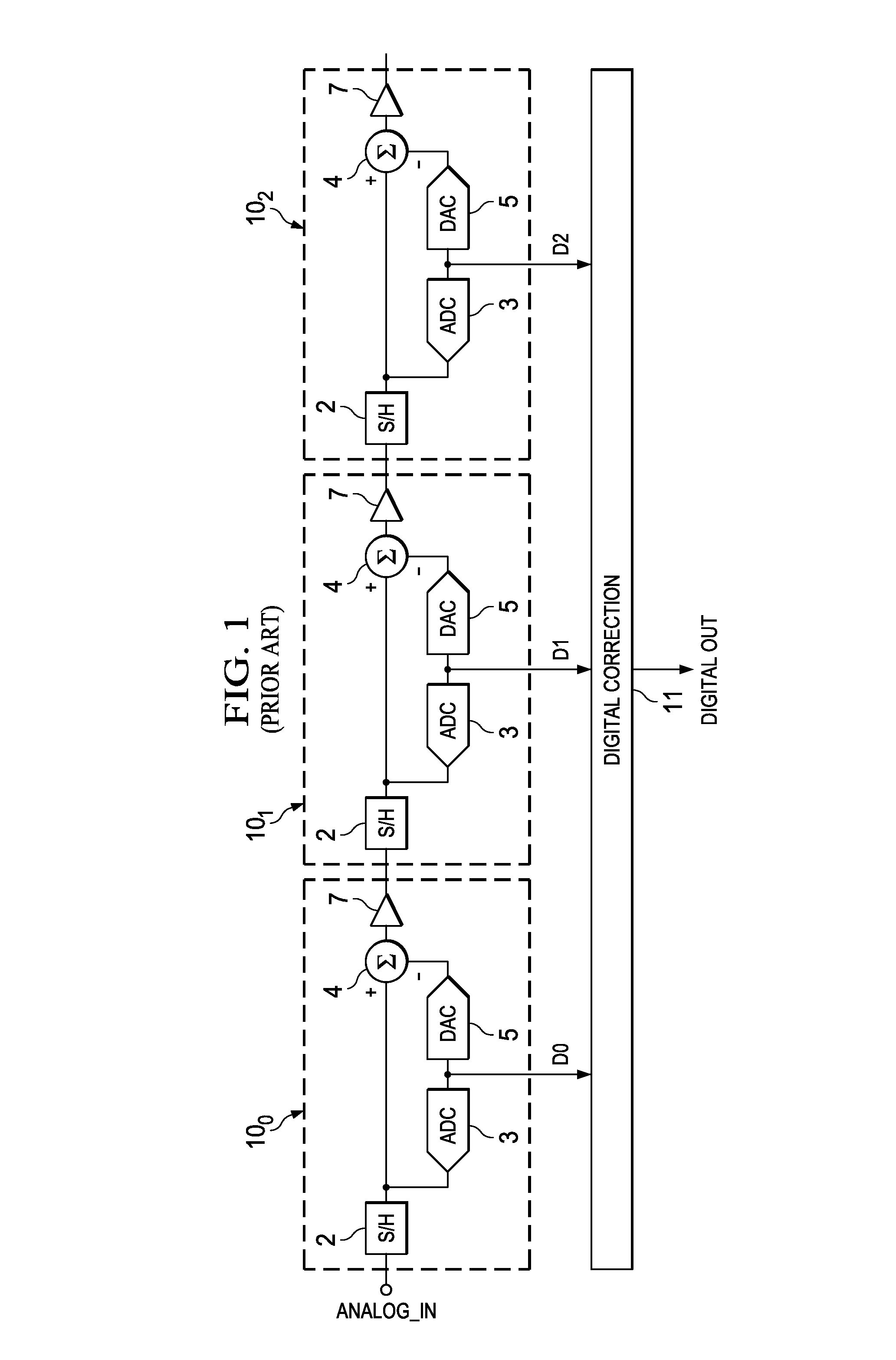
In order to improve the error correction performance, however, the designer must either increase the number of pipeline stages, or increase the number of digital bits produced by each stage, either of which increases the circuit complexity and thus the cost, and may decrease the sample rate performance of the circuit.
As known in the art, systematic error is error inherent in the particular circuit realization of the ADC function.
However, the dithering technique necessarily introduces additional overhead circuitry into the analog interface, specifically by the circuitry required to inject the random noise into the input signal path.
However, the non-linear compensation function necessarily inserts significant computational burden on the digital circuitry, as evident by the necessity of a digital signal processor to derive and apply that compensation.

Method used


Image

  • Digital error correction in an analog-to-digital converter
  • Digital error correction in an analog-to-digital converter
  • Digital error correction in an analog-to-digital converter

Examples


Embodiment Construction

[0026]The present invention will be described in connection with its embodiments, namely as analog-to-digital converters according to various implementations. It is to be understood that the following description is provided by way of example only, and is not intended to limit the true scope of this invention as claimed.

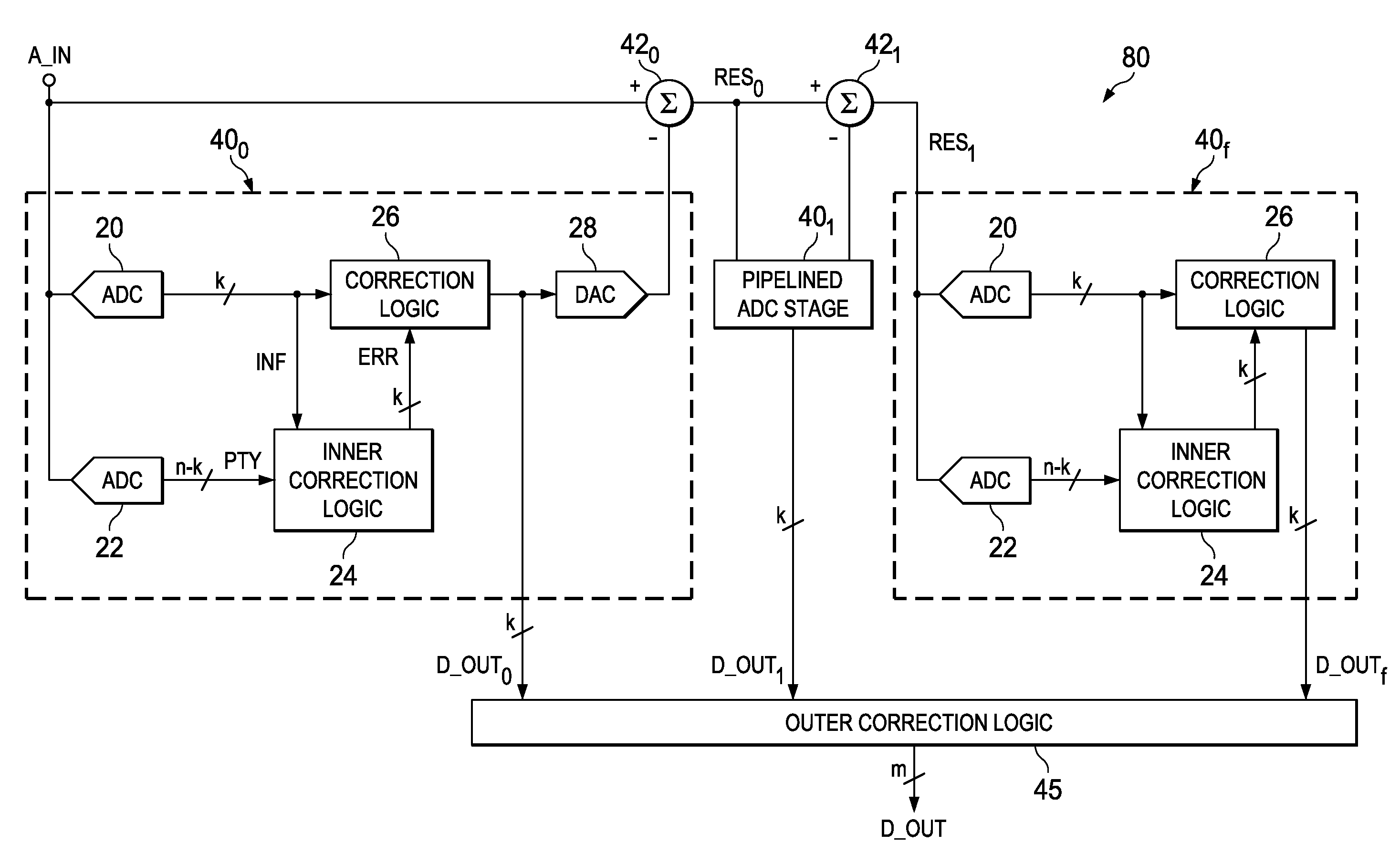
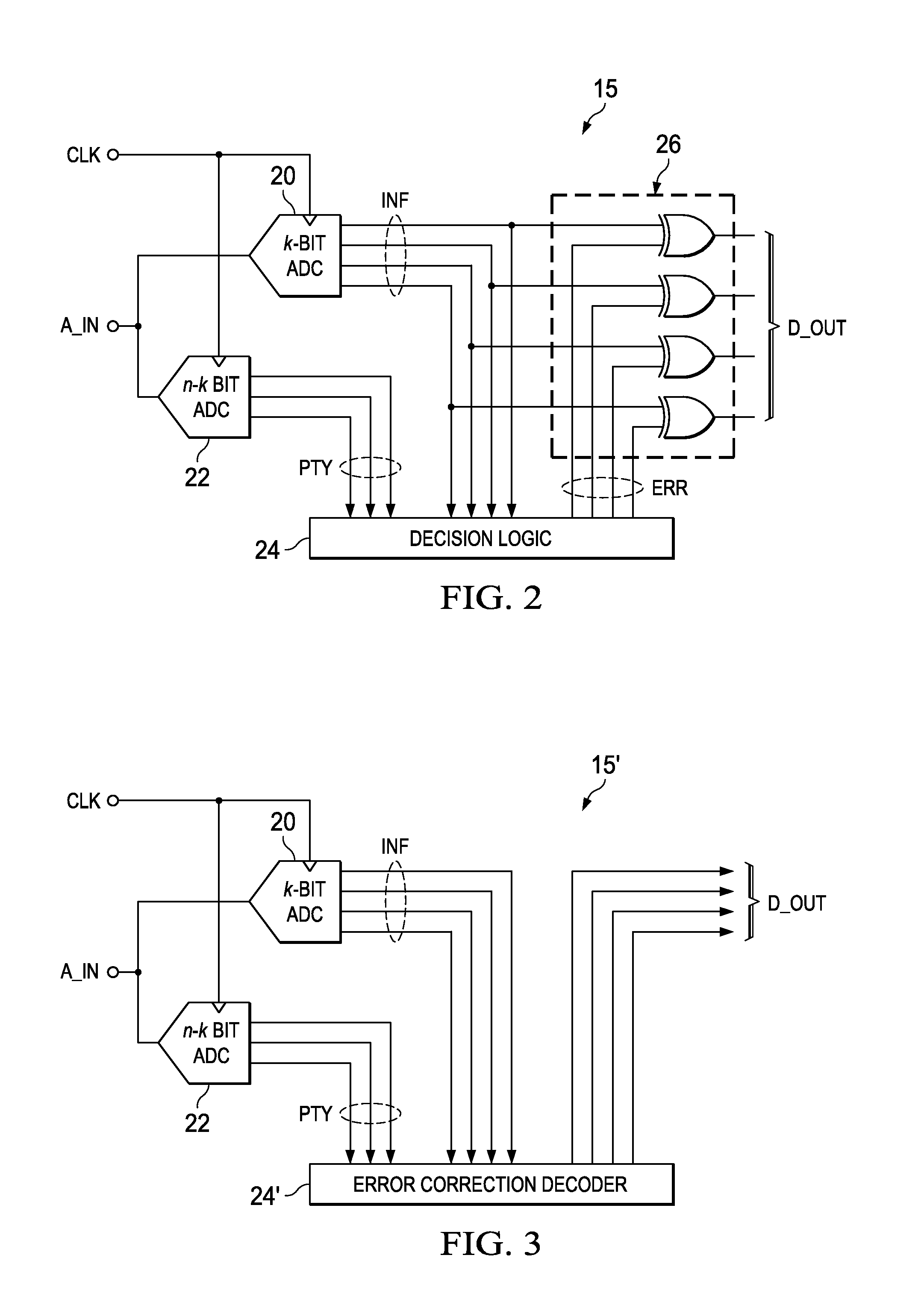
[0027]Referring now to FIG. 2, the construction and operation of analog-to-digital converter (ADC) 15 according to an embodiment of the invention will be described. ADC 15 according to this embodiment of the invention may serve as a stand-alone ADC circuit, for example as realized as a separate integrated circuit, or as a single-stage ADC circuit within a larger scale integrated circuit such as a single-chip communications or processing circuit as now commonly available, or as a stage in a pipelined ADC circuit, an example of which will be described in further detail below. It is contemplated that those skilled in the art having reference to this specification will b...


PUM


Abstract

An analog-to-digital converter (ADC) function in which digital error correction is provided. Parallel ADC stages are synchronously clocked to convert an analog input signal into digital words; at least one of the digital outputs is encoded according to an error correction code. Decision logic circuitry decodes a code word comprised of the concatenation of the digital outputs from the parallel stages, to derive a digital output from which the digital output word corresponding to the analog input signal can be derived. The decision logic circuitry can provide an error signal used to correct the state of one or more bits of the digital output from one of the ADC stages, for the case of a systematic code; alternatively, the decision logic circuitry can directly decode the code word to provide the digital output. The architecture may be applied to stages in a pipelined ADC.

Description

CROSS-REFERENCE TO RELATED APPLICATIONS[0001]Not applicable.STATEMENT REGARDING FEDERALLY SPONSORED RESEARCH OR DEVELOPMENT[0002]Not applicable.BACKGROUND OF THE INVENTION[0003]This invention is in the field of analog-to-digital converter circuits. Embodiments of this invention are directed to error correction and compensation in such circuits.[0004]Despite the continuing trend toward the digitization of electronic circuits and systems over recent years, modern electronic systems must still often process and generate electrical signals in the analog domain. For example, analog signals are transmitted and received in many modern communications technologies, and analog signals are used in instrumentation and control systems. Data converter circuits are therefore required to provide an interface between the digital and analog domains, especially in those systems in which digital signal processing is applied. As is fundamental in the art, analog-to-digital converters (ADCs) convert anal...

Claims


Application Information

Patent Timeline
Patent Type & Authority Patents(United States)
IPC IPC(8): H03M1/06
CPCH03M1/0687H03M1/167
Inventor MILLER, JOHN EARLEPAYNE, ROBERT FLOYD
Owner TEXAS INSTR INC
Learn More