Internal electrical contact for enclosed MEMS devices

a technology of electrical contact and mems device, which is applied in the manufacture of microstructural devices, electrical apparatus, and semiconductor devices, etc., can solve the problems of increasing the overall thickness of the mems device when packaged, and the need for vertical space for the wire bond to be completed, so as to reduce the thickness of the device

Active Publication Date: 2013-10-22
INVENSENSE
View PDF21 Cites 40 Cited by
  • Summary
  • Abstract
  • Description
  • Claims
  • Application Information

AI Technical Summary

Benefits of technology

[0005]Accordingly, a MEMS device in accordance with an embodiment provides an internal electrical connection and eliminates the need for an external wire bond for grounding needed in conventional MEMS devices and may reduce the device thickness. Other aspects and advantages of the present invention will become apparent from the following detailed description, taken in conjunction with the accompanying drawings, illustrating by way of example the principles of the invention.

Problems solved by technology

However, the wire bond requires vertical space and increases overall thickness of the MEMS device when packaged.

Method used


Image

  • Internal electrical contact for enclosed MEMS devices
  • Internal electrical contact for enclosed MEMS devices
  • Internal electrical contact for enclosed MEMS devices

Examples


first embodiment

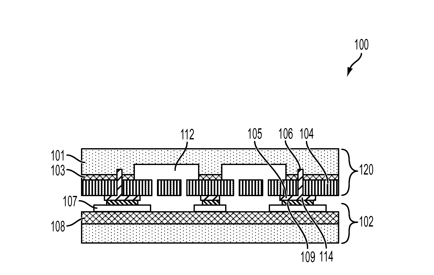
[0016]FIG. 1 is a diagram which illustrates a cross-section of the bonded MEMS-base substrate device with an internal direct electric coupling in accordance with a An engineered silicon-on-insulator (ESOI) substrate 120 includes a handle layer 101 with cavities 112 and a device layer 104, fusion bonded together with a thin dielectric film 103 (such as silicon oxide) in between the device layer 104 and handle layer 101. An electrical connection between the handle layer 101 and the device layer 104 may be achieved by etching one or more vias 106 through the device layer 104 and the thin dielectric layer 103 into the handle layer 101 and by filling the vias 106 with a conductive material 114, such as polysilicon, tungsten, titanium, titanium nitride, aluminum, or germanium. The MEMS substrate is considered complete after a germanium (Ge) 109 and standoffs 105 comprising conductive material 114 are formed and MEMS actuator structures are patterned and etched in device layer 104. Altern...

second embodiment

[0020]FIG. 3 is a diagram which illustrates a cross-section of the bonded MEMS-base substrate device with an internal direct electric coupling in accordance with a In this embodiment, the electric coupling path is formed from handle layer 201 to MEMS device layer 204, across dielectric film 203, and eventually to base substrate Al pad 207 after MEMS to base substrate AlGe eutectic bonding.

[0021]An ESOI substrate 220 is comprised of a handle layer 201 with cavities 212 and a device layer 204, fusion bonded together with a thin dielectric layer 203 (such as silicon oxide) in between the device layer 204 and handle layer 201. The ESOI substrate is completed after device layer thinning. An electrical connection between handle layer 201 and device layer 204 can be achieved by etching at least one via 206 at any locations through device layer 204 and thin dielectric layer 203 into or exposing the surface of handle layer 201 and filling the via 206 by conductive materials, such as polysil...

third embodiment

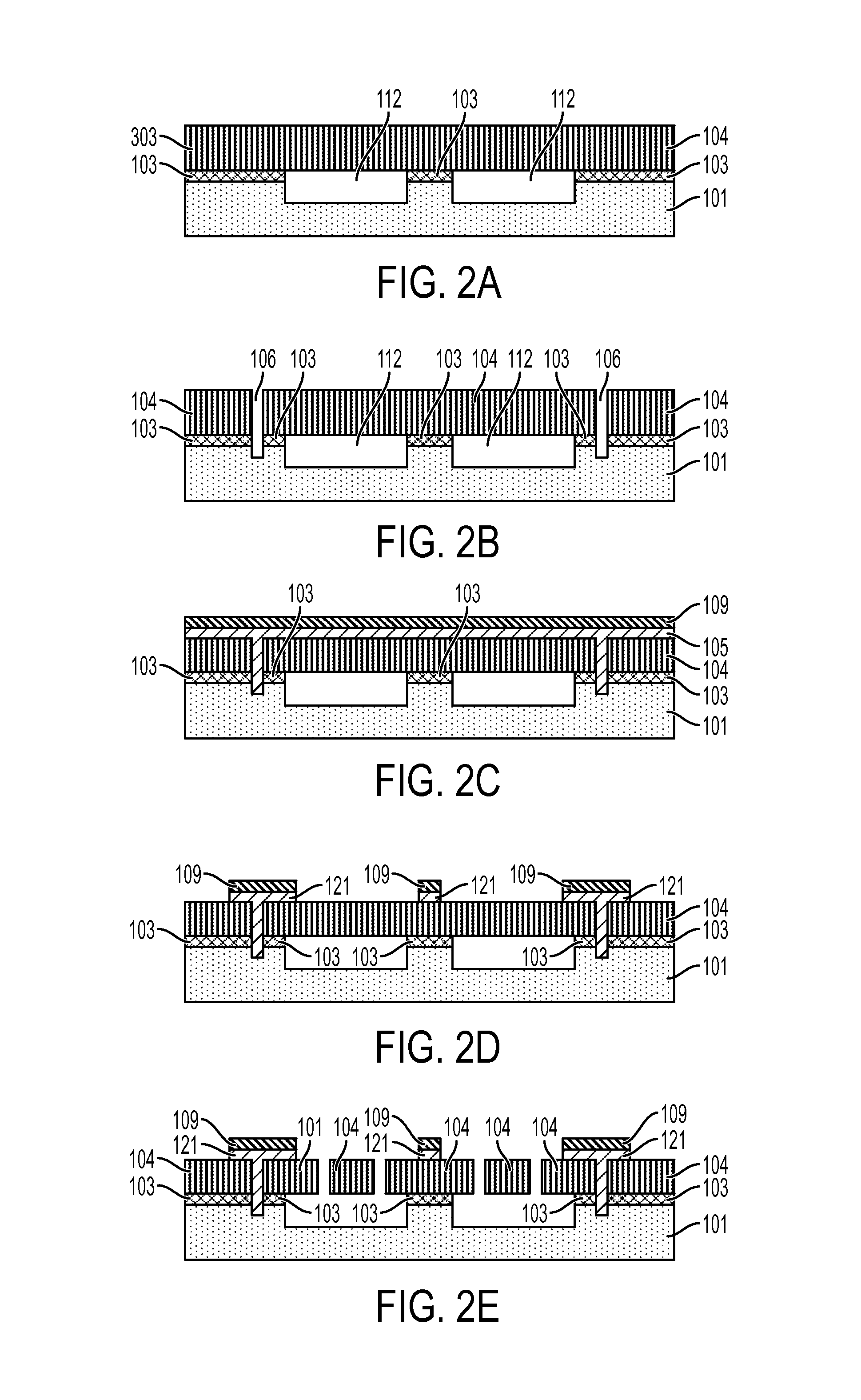
[0023]FIG. 4 is a diagram illustrating the electric coupling between handle layer 301. MEMS device layer 304, and base substrate 302 using polysilicon for the device layer 304 and AlGe eutectic bonding. The process flow and fabrication method of MEMS substrate using a surface micro-machining process technique are illustrated in FIGS. 5A-5F. FIGS. 5A-5F are diagrams which illustrate a series of cross-sections illustrating processing steps to build the electric coupling from handle layer 301 to device layer 306 ready to bond to a base substrate 302 for the device of FIG. 4. Starting from FIG. 5A, a thin dielectric layer 303 (typically silicon oxide) is deposited on a handle layer 301. Thereafter the layer 303 is patterned and etched to form vias 312. A silicon layer 306 (FIG. 5B) is deposited onto the handle layer 301 followed by thinning and planarization, (for example grinding or chemical mechanical polishing) to desired device layer thickness. FIG. 50 illustrates an embodiment with...


PUM


Abstract

A MEMS device is disclosed. The MEMS device comprises a MEMS substrate. The MEMS substrate includes a first semiconductor layer connected to a second semiconductor layer with a dielectric layer in between. MEMS structures are formed from the second semiconductor layer and include a plurality of first conductive pads. The MEMS device further includes a base substrate which includes a plurality of second conductive pads thereon. The second conductive pads are connected to the first conductive pads. Finally, the MEMS device includes a conductive connector formed through the dielectric layer of the MEMS substrate to provide electrical coupling between the first semiconductor layer and the second semiconductor layer. The base substrate is electrically connected to the second semiconductor layer and the first semiconductor layer.

Description

FIELD OF THE INVENTION[0001]The present invention relates generally to MEMS devices and more specifically to providing electric contact of the enclosure of the MEMS devices.BACKGROUND[0002]MEMS devices are utilized in a variety of environments. In such devices a handle layer is normally required to be electrically grounded to provide an electric shield for low noise performance. The electrical connection to the handle layer is provided by a wire bond. However, the wire bond requires vertical space and increases overall thickness of the MEMS device when packaged. Accordingly, what is desired is a MEMS device and method where the wire bond is not necessary.[0003]The MEMS device and method for providing electrical connection to the handle layer should be simple, easily implemented and adaptable to existing environments. The present invention addresses such a need.SUMMARY OF THE INVENTION[0004]A MEMS device is disclosed. The MEMS device comprises a MEMS substrate. The MEMS substrate inc...

Claims


Application Information

Patent Timeline
Patent Type & Authority Patents(United States)
IPC IPC(8): H01L27/14
CPCB81B7/0064B81C1/00269B81C1/00301B81C2203/0118B81C2203/019B81B2207/098B81C2203/031
Inventor HUANG, KEGANGSHIN, JONGWOOLIM, MARTINDANEMAN, MICHAEL J.SEEGER, JOSEPH
Owner INVENSENSE
Why Eureka
Try Eureka