Lead frame and method for manufacturing the same

a semiconductor and lead frame technology, applied in the direction of superimposed coating process, resistive material coating, liquid/solution decomposition chemical coating, etc., can solve the problem of increasing the cost of semiconductor package production by the pre-plating method, and achieve the effect of improving or enhancing the performance of the semiconductor package, reducing the thickness of high-priced metal, and low production cos

Inactive Publication Date: 2013-10-22
ALS
View PDF19 Cites 9 Cited by
  • Summary
  • Abstract
  • Description
  • Claims
  • Application Information

AI Technical Summary

Benefits of technology

[0012]The present invention provides a lead frame and a method for manufacturing the lead frame, and provide a method for decrease a thickness of high-priced metal used in a pre-plating method for manufacturing a lead frame.
[0013]Also, the present invention provides a method for improving or enhancing performance of the semiconductor package including a lead frame at a low cost of production.
[0014]Further, the present invention provides a lead frame advanced in wire-bonding strength, solerability, mold compound adhesion, and lamination quality.

Problems solved by technology

However, since a lead frame is plated with high-priced metals, cost of production for semiconductor package manufactured by the pre-plating method increases.

Method used


Image

  • Lead frame and method for manufacturing the same
  • Lead frame and method for manufacturing the same

Examples


Embodiment Construction

[0018]The invention shows a lead frame and a manufacturing method of the lead frame. Although manufactured at low cost of production, the lead frame according to an embodiment of the invention includes advanced electronic or mechanical properties. While the invention will be described in conjunction with exemplary embodiments, it will be understood that present description is not intended to limit the invention to those exemplary embodiments. On the contrary, the invention is intended to cover not only the exemplary embodiments, but also various alternatives, modifications, equivalents and other embodiments, which may be included within the spirit and scope of the invention as defined by the appended claims.

[0019]Hereinafter reference will now be made in detail to various embodiments of the present invention, examples of which are illustrated in the accompanying drawings and described below.

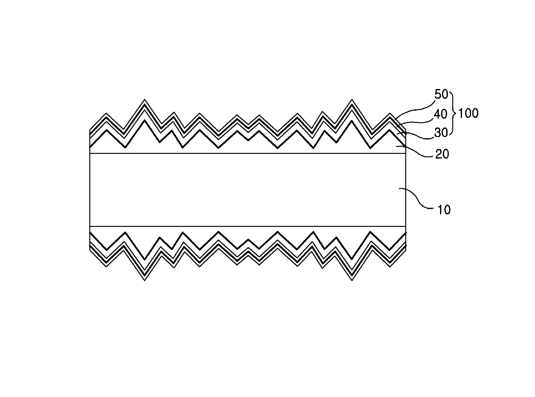
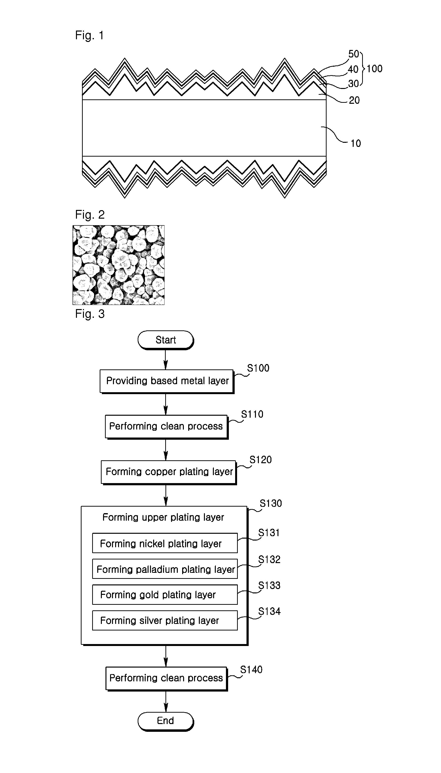
[0020]FIG. 1 is a cross-sectional view describing a lead frame according to an embodiment of ...


PUM

PropertyMeasurementUnit
Raaaaaaaaaaa
thicknessaaaaaaaaaa
thicknessaaaaaaaaaa

Abstract

A lead frame comprises: a base metal layer; a copper plating layer, including one of a copper layer and an alloy layer including a copper, configured to plate the based metal layer to make a surface roughness; and an upper plating layer, including at least one plating layer including at least one selected from the group of a nickel, a palladium, a gold, a silver, a nickel alloy, a palladium alloy, a gold alloy, and a silver alloy, configured to plate the copper plating layer.

Description

CROSS-REFERENCE TO RELATED APPLICATIONS[0001]This application is the U.S. national stage application of International Patent Application No. PCT / KR2010 / 001098, filed Feb. 23, 2010, which claims priority to Korean Application No. 10-2009-0021371, filed Mar. 12, 2009, the disclosures of each of which are incorporated herein by reference in their entirety.TECHNICAL FIELD[0002]The present invention relates to a lead frame for a semiconductor package and a method for manufacturing the lead frame, and more particularly, to a lead frame for a semiconductor package which can maintain or raise a quality of the semiconductor package at a low cost of production.BACKGROUND ART[0003]A lead frame like a semiconductor chip is one of components included in a semiconductor package. The lead frame serves as both a wire for connecting the semiconductor chip to an external circuit and a supporting form for mounting the semiconductor chip and fixing the same at a static state.[0004]A conventional lead f...

Claims


Application Information

Patent Timeline
Patent Type & Authority Patents(United States)
IPC IPC(8): H01L23/495H01L21/00
CPCH01L23/49582H01L24/48H01L2224/85444H01L2924/01046H01L2924/01078H01L2924/01079H01L2924/00014H01L2224/45099H01L2224/48H01L2224/85439H01L23/495
Inventor CHO, IN KUKPARK, KYOUNG TAEKKWAK, SANG SOOKIM, EUN JINSON, JIN YOUNGPARK, CHANG HWA
Owner ALS
Why Eureka
Try Eureka