Very dense NVM bitcell

a bitcell, very dense technology, applied in the direction of instrumentation, cad circuit design, computer aided design, etc., can solve the problems of increasing the cost of producing the bitcell and possibly changing the performance or characteristics of the produced device, so as to reduce the size, enhance the capacitive coupling of source-floating gate, and reduce the effect of siz

Active Publication Date: 2013-12-03
SYNOPSYS INC
View PDF18 Cites 5 Cited by
  • Summary
  • Abstract
  • Description
  • Claims
  • Application Information

AI Technical Summary

Benefits of technology

[0006]Embodiments relate to a nonvolatile memory (“NVM”) bitcell with reduced size and enhanced capacitive coupling between the source and the floating gate. The bitcell may use band to band tunneling, channel hot injection impact ionized hot electron injection, and / or enhanced source-floating gate capacitive coupling to read, write, or erase the bitcell.

Problems solved by technology

Currently, eFLASH has a very small bitcell, but requires steps in addition to the standard CMOS process, which increases the cost of producing the bitcell and possibly changes the performance or characteristics of the produced devices.
EEPROM is compatible with standard CMOS processes, but has a relatively large bitcell size, and thus is only suitable for low bit count memories.

Method used


Image

  • Very dense NVM bitcell
  • Very dense NVM bitcell
  • Very dense NVM bitcell

Examples


example embodiments

General Overview of Example Embodiments

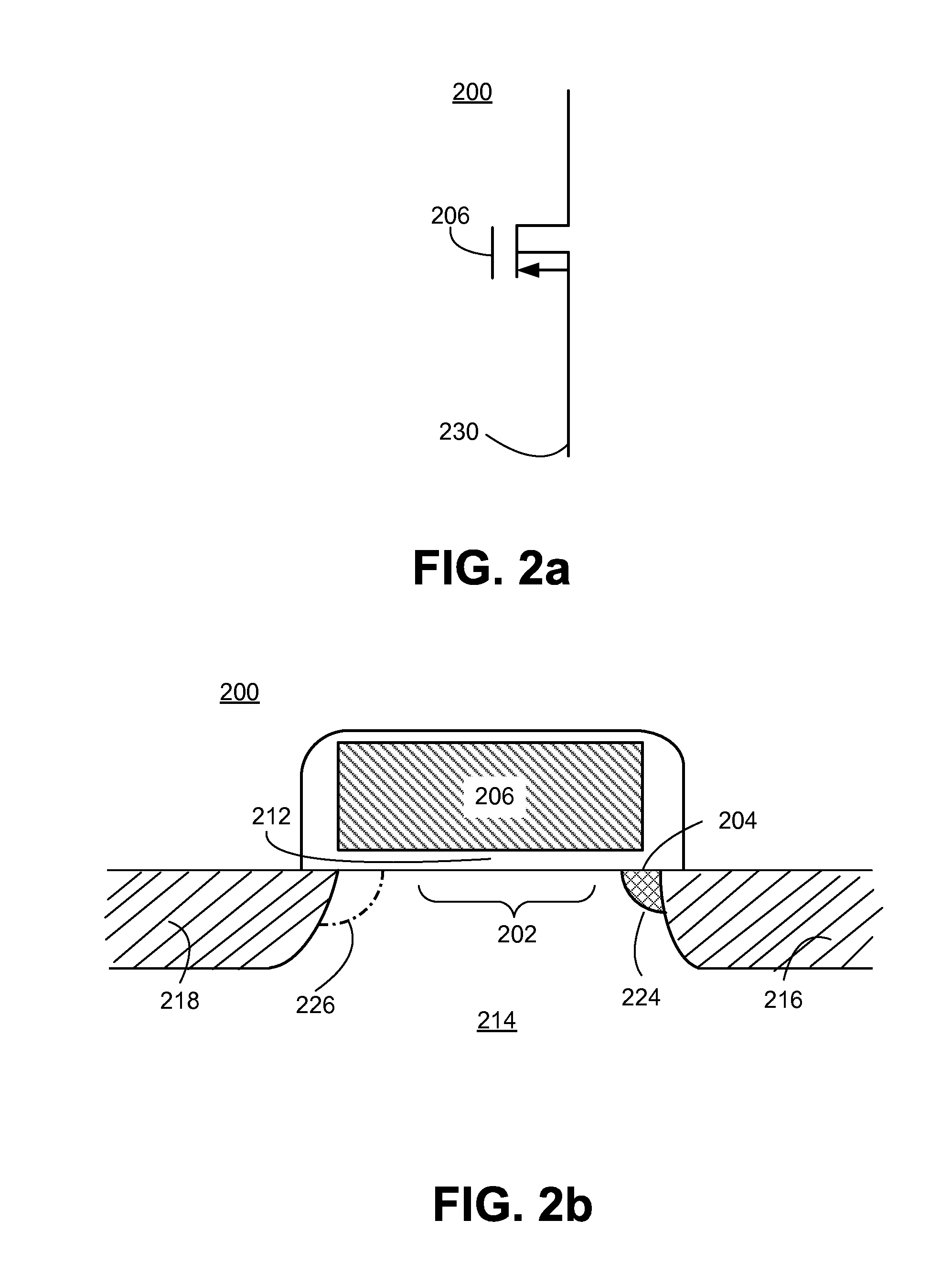
[0025]Embodiments save space compared to conventional NVM bitcells, in part, by removing the select transistor and 104 and erase transistor 114. The selection and erasure mechanism may instead be integrated into the memory transistor 108 itself, through specialized design of the physical layout of the memory transistor 108.

[0026]FIG. 2a is a circuit diagram of a NVM bitcell 200 according to one embodiment. The NVM bitcell 200 of FIG. 2a saves space over conventional NVM bitcells (i.e. it is more dense), because all functions of the bitcell have been incorporated into a single memory transistor 200. In the description of FIG. 1 above, it was useful to distinguish the bitcell from the transistors that made up the bitcell, because there was more than one transistor in each bitcell circuit. In contrast, the terms “NVM bitcell” and “memory transistor” may be used interchangeably in embodiments described below with reference to FIGS. 2a through 5b be...

example layout

Created with One Additional Mask Step

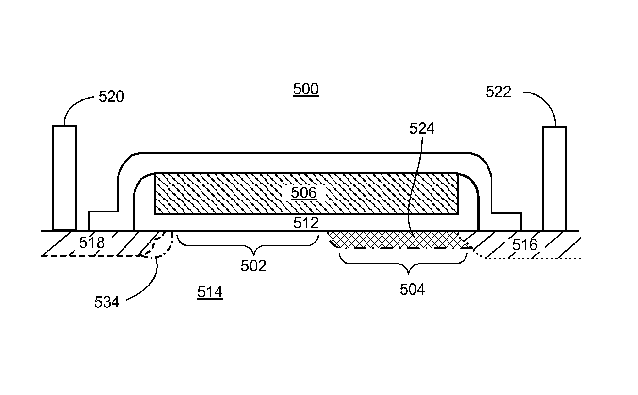
[0053]FIG. 5a is a plan view of a NVM bitcell 500 according to one embodiment. The NVM bitcell 500 with a second layout can be is fabricated using the standard CMOS process, plus one additional mask step. In the CMOS process, the additional mask step is added before the floating gate oxide 512 or floating gate 506 is added on top of the well 514. The second layout also increases the capacitive coupling between source 516 and floating gate 506. In a P-type embodiment, the NVM bitcell 500 includes a rectangular floating gate 506 that sits on top of a N-well 514. In a N-type embodiment, the NVM bitcell includes a P-well instead.

[0054]In one embodiment, the N-well 514 sits beneath the entirety of device 500 (not shown in FIG. 5a, see FIG. 5b) The bitcell 500 has asymmetric doping between the source 516 and the drain 518. The source region 516 extends partway underneath the floating gate 506 on the side of the floating gate 506 closest to the source c...


PUM


Abstract

An asymmetric non-volatile memory bitcell is described. The bitcell comprises source and drain regions comprising carriers of the same conductivity type. A floating gate rests on top of the well, and extends over a channel region, and at least a portion of the source and drain regions. The drain region comprises additional carriers of a second conductivity type, allowing band to band tunneling. The source region comprises additional carriers of a first conductivity type, thereby increasing source-gate capacitance. Thus, the bitcell incorporates a select device, thereby decreasing the overall size of the bitcell. The bitcell may be created without any additional CMOS process steps, or through the addition of a single extra mask step.

Description

BACKGROUND[0001]1. Field of Art[0002]This disclosure generally relates to the field of nonvolatile memory, particularly non volatile memory bitcell layouts.[0003]2. Description of the Related Art[0004]Nonvolatile memory (NVM) refers to memory that persistently stores information bits when not powered. A nonvolatile memory bitcell (NVM bitcell) stores a single bit of data. Some types of NVM bitcells are implemented using transistors with floating gates. The amount of charge residing on a floating gate determines whether the bitcell is storing a logical “1” or a logical “0”. The floating gate is referred to as “floating” because the floating gate is electrically isolated from the surroundings by an oxide or dielectric.[0005]In order to expand applications and reduce costs of memory devices, it is desirable to accommodate a large number of bitcells in a given area. It is also desirable to decrease the cost of fabricating each bitcell by using standard complementary metal-oxide-semicond...

Claims


Application Information

Patent Timeline
Patent Type & Authority Patents(United States)
IPC IPC(8): H01L21/02
CPCH01L29/42324H01L29/66825H01L29/7885G06F17/5068G11C16/10H01L29/788G06F30/39
Inventor HORCH, ANDREW E.
Owner SYNOPSYS INC
Why Eureka
Try Eureka