Semiconductor device and semiconductor package

a semiconductor and semiconductor technology, applied in the direction of semiconductor devices, semiconductor/solid-state device details, diodes, etc., can solve the problem of difficult reduction of forward voltage (vf) and achieve the effect of increasing the dc resistance and withstanding voltage of schottky barrier diodes

Active Publication Date: 2013-12-17
ROHM CO LTD
View PDF3 Cites 6 Cited by
  • Summary
  • Abstract
  • Description
  • Claims
  • Application Information

AI Technical Summary

Benefits of technology

[0008]To ensure a (certain) withstand voltage of a transistor, the thickness of an n-type semiconductor layer is required to be greater than a necessary thickness. In the semiconductor device of Patent Document 1, the thickness of the n-type semiconductor layer in the area where the transistor is formed is the same as the area where a Schottky barrier diode is formed. Therefore, although the withstand voltage of the transistor is guaranteed, the thickness of the n-type semiconductor layer in the Schottky barrier diode area is required to be higher than a necessary thickness, so the DC resistance of the Schottky barrier diode increases. Therefore, a forward voltage (VF) of a Schottky barrier diode is difficult to reduce.
[0009]Therefore, the present invention is directed to providing a semiconductor device capable of ensuring a withstand voltage of a transistor and reducing a forward voltage of a Schottky barrier diode in a package with the transistor and the Schottky barrier diode formed on a chip, and a semiconductor package formed by a resin package covering the semiconductor device.
[0014]According to the present composition, a minimum level withstand voltage of the Schottky barrier diode can be ensured.
[0016]According to the present composition, the steps of forming the first trench and polishing the semiconductor layer in the diode area from the surface side to make the semiconductor layer thinner may be carried out in one step. Reducing the number of steps lowers the cost of fabricating the semiconductor device. In this manner, an inexpensive high-performance semiconductor device can be provided.
[0024]When the transistor of the transistor area is ON, the Schottky barrier diode of the diode area is OFF, thereby realizing heat dissipation of the semiconductor layer by using the diode area. When the transistor is OFF, heat dissipation of the semiconductor layer may be realized by using the transistor area. The above manner may prevent the temperature of the semiconductor device from rising. In particular, the transistor area is configured to surround the diode area, so as to dissipate the heat of one area by means of another area, thereby effectively preventing the temperature of the semiconductor device from rising. When multiple diode areas exist, the diode areas are scattered and uniformly distributed at a necessary interval, thus further effectively preventing the temperature of the semiconductor device from rising.

Problems solved by technology

Therefore, a forward voltage (VF) of a Schottky barrier diode is difficult to reduce.

Method used


Image

  • Semiconductor device and semiconductor package
  • Semiconductor device and semiconductor package
  • Semiconductor device and semiconductor package

Examples


Embodiment Construction

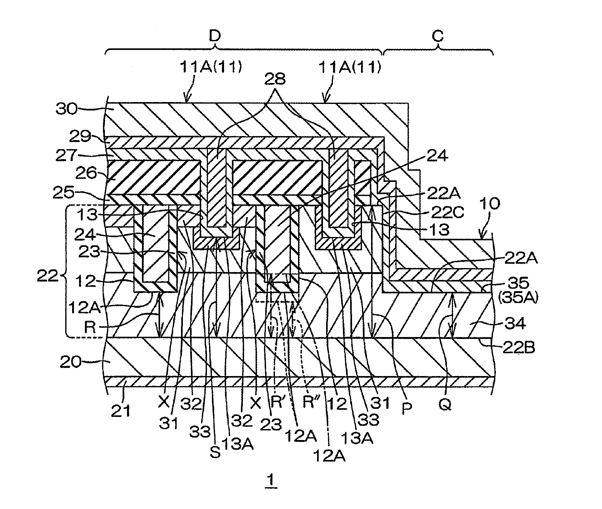
[0075]Hereinafter, the embodiments of the present invention will be illustrated in detail with reference to the drawings.

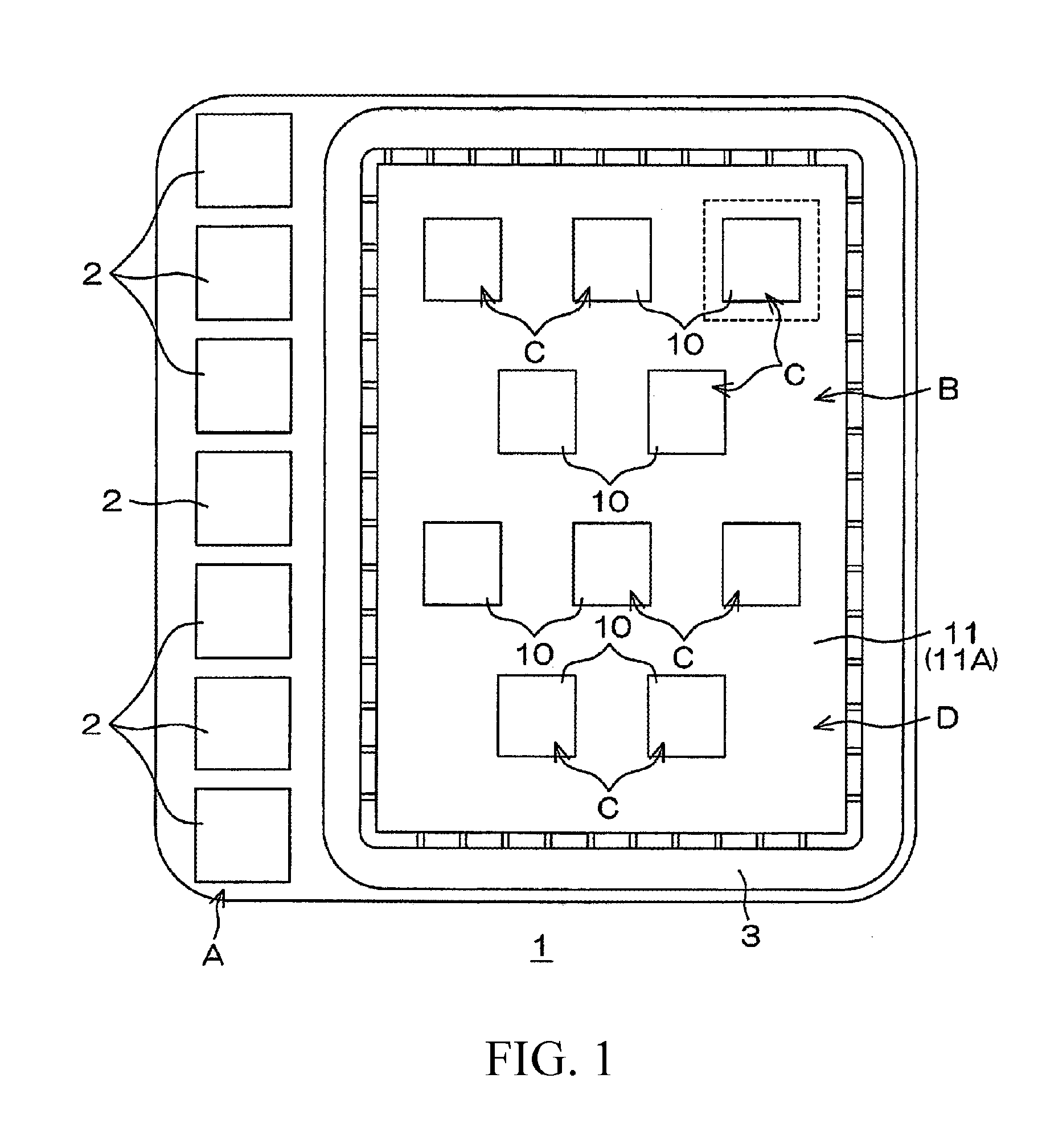
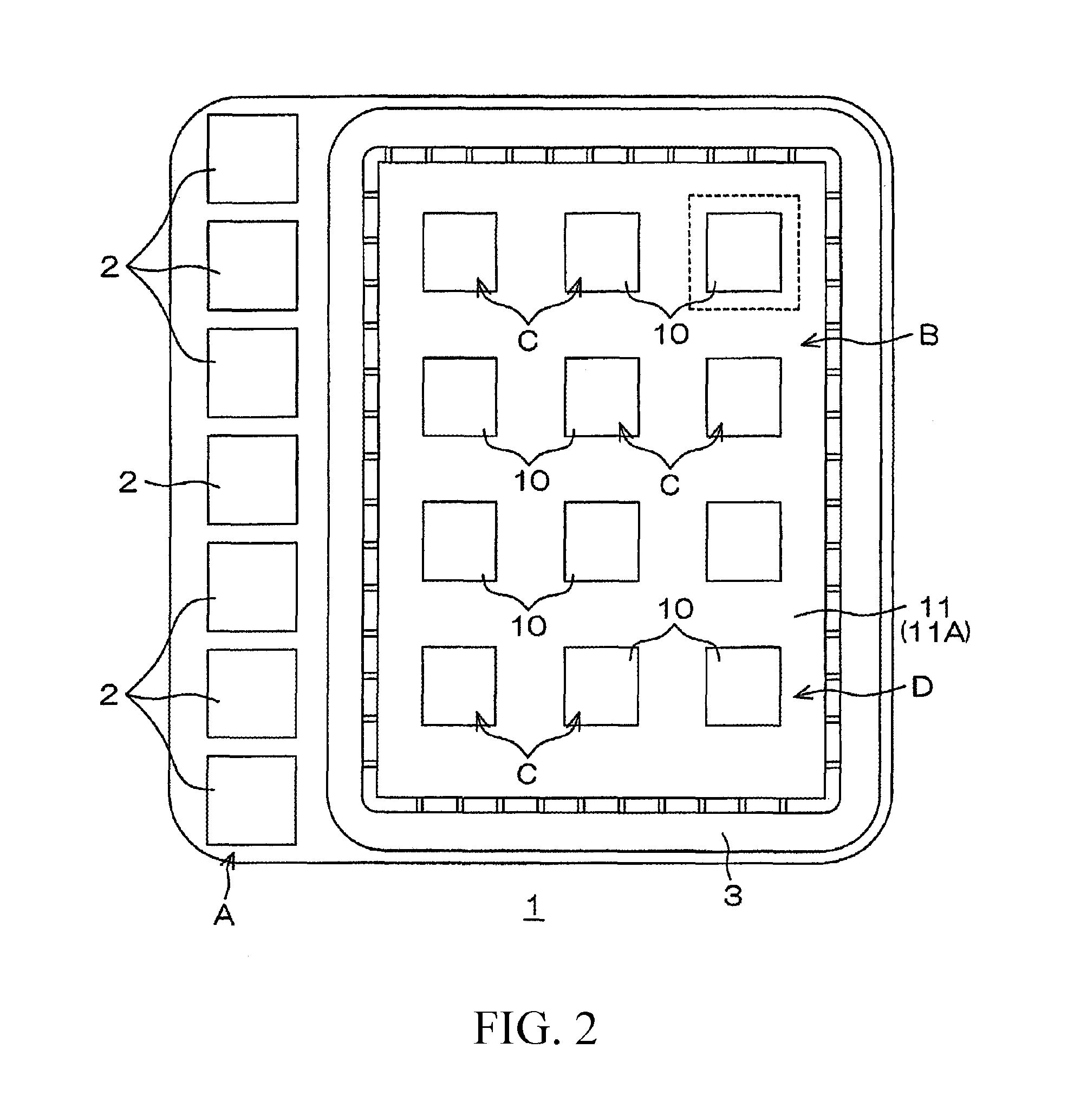
[0076]FIG. 1 is a schematic plan view of a semiconductor device according to an embodiment of the present invention. FIG. 2 is a schematic plan view of a semiconductor device according to another embodiment of the present invention.

[0077]In an embodiment of the present invention, the semiconductor device 1 is in the shape of a quadrilateral chip when observed from the top. Each of four sides of the semiconductor device 1 when observed from the top has a length for example of several millimeters.

[0078]On the quadrilateral surface of the semiconductor device 1 when observed from the top, an external connection area A is formed along one side, and a movable area B is formed in the area outside the external connection area A. The semiconductor device 1 has: a plurality of external electrodes 2 configured in the external connection area A; a retaining ring 3 surroundin...


PUM


Abstract

A semiconductor device capable of ensuring a withstand voltage of a transistor and reducing a forward voltage of a Schottky barrier diode in a package with the transistor and the Schottky barrier diode formed on chip, and a semiconductor package formed by a resin package covering the semiconductor device are provided. The semiconductor device 1 includes a semiconductor layer 22, a transistor area D formed on the semiconductor layer 22 and constituting the transistor 11, and a diode area C formed on the semiconductor layer 22 and constituting the Schottky barrier diode 10. The semiconductor layer 22 in the diode area C is thinner than the semiconductor layer 22 in the transistor area D.

Description

BACKGROUND OF THE INVENTION[0001]1. Field of the Invention[0002]The present invention relates to a semiconductor device and a semiconductor package formed by a resin package covering the semiconductor device.[0003]2. Description of the Related Art[0004]The semiconductor device disclosed in Patent Document 1 contains a Schottky barrier diode connected between a source and a drain. In particular, a p-type base layer is formed on a surface portion of an n-type semiconductor layer stacked on an n-type semiconductor substrate of the semiconductor device. A trench is dug from the surface of the n-type semiconductor layer and penetrates through the p-type base layer, and a gate insulating film is formed on the sidewall and the bottom of the trench. A gate electrode is embedded in the trench. An n-type diffusion layer is formed on the surface portion of the p-type base layer.[0005]A trench gate-type transistor is thereby formed in the semiconductor device. In the transistor, the n-type diff...

Claims


Application Information

Patent Timeline
Patent Type & Authority Patents(United States)
IPC IPC(8): H01L27/01
CPCH01L23/49562H01L27/0629H01L29/0657H01L29/66727H01L29/66734H01L29/7806H01L29/7813H01L27/0255H01L27/0727H01L29/41766H01L29/456H01L29/47H01L29/872H01L2224/48091H01L2224/48247H01L2224/48465H01L2924/00014H01L24/48H01L2924/01019H01L2924/13091H01L2924/00H01L23/3107H01L24/49H01L2224/49175H01L2924/12032H01L2924/181H01L2224/05553H01L2224/49113H01L2924/00012H01L2224/45099H01L2224/45015H01L2924/207H01L23/293H01L29/4236
Inventor KENICHI, YOSHIMOCHI
Owner ROHM CO LTD
Why Eureka
Try Eureka