

Laser formation of graphene
a technology of graphene and laser, which is applied in the direction of solid-state diffusion coating, semiconductor/solid-state device details, coatings, etc., can solve the problems of metal compatibility difficulties with high-temperature ceramic materials such as aluminum nitride (aln) and silicon carbide (sic), not fully solved, and the thermal expansion coefficient is not high enough
- Summary
- Abstract
- Description
- Claims
- Application Information
AI Technical Summary
Benefits of technology
Problems solved by technology
Method used
Image

Examples
first embodiment
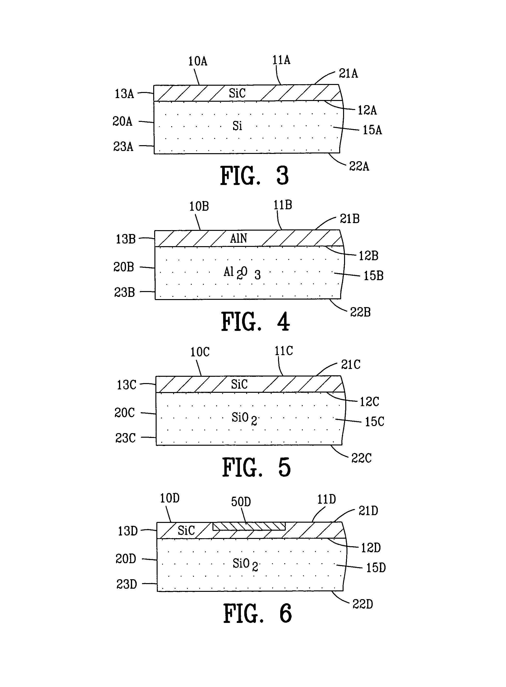
[0070]FIG. 3 is an enlarged sectional view of the invention illustrating a wide bandgap material 10A formed in the substrate 20A. In this example, the non-wide bandgap material 15A of the substrate 20A is a silicon (Si) material whereas the wide bandgap material 10A is silicon carbide (SiC).
[0071]The silicon (Si) non-wide bandgap material 15A is converted into the silicon carbide (SiC) wide bandgap material 10A as the thermal energy beam 40 scans across the first surface 21A of the substrate 20A. The thermal energy beam 40 scans across the first surface 21A of the substrate 20A in an atmosphere of methane gas or acetylene gas. The thermal energy beam 40 heats the silicon atoms of the non-wide bandgap material 15A. The heated silicon atoms of the non-wide bandgap material 15A react with the carbon atoms of the methane gas or acetylene gas atmosphere to create the silicon carbide (SiC) wide bandgap material 10A.
second embodiment
[0072]FIG. 4 is an enlarged sectional view of the invention illustrating a wide bandgap material 10B formed in the substrate 20B. In this example, the non-wide bandgap material 15B of the substrate 20B is aluminum oxide (Al2O3) material whereas the wide bandgap material 10B is aluminum nitride (AlN).
[0073]The aluminum oxide (Al2O3) non-wide bandgap material 15B is converted into the aluminum nitride (AlN) wide bandgap material 10B as the thermal energy beam 40 scans across the first surface 21B of the substrate 20B. The thermal energy beam 40 scans across the first surface 21B of the substrate 20B in an atmosphere of nitrogen to create the aluminum nitride (AlN).
[0074]Gallium arsenide (GaAs) non-wide bandgap material (thermal conductivity 55 W / m-K) is converted to gallium nitride (GaN) wide bandgap material (thermal conductivity 130 W / m-K) by this method shown for converting aluminum oxide to aluminum nitride.
[0075]Typically, the formation of aluminum nitride (AlN) is not chemical a...
third embodiment
[0077]FIG. 5 is an enlarged sectional view of the invention illustrating a wide bandgap material 10C formed in the substrate 20C. In this example, the non-wide bandgap material 15C of the substrate 20C is a silica (SiO2) material whereas the wide bandgap material 10C is silicon carbide (SiC).
[0078]The silica (SiO2) non-wide bandgap material 15C is converted into the silicon carbide (SiC) wide bandgap material 10C as the thermal energy beam 40 scans across the first surface 21C of the substrate 20C. The thermal energy beam 40 scans across the first surface 21C of the substrate 20C in an atmosphere of methane gas or acetylene gas. The thermal energy beam 40 heats the silicon atoms of the non-wide bandgap material 15C. The heated silicon atoms of the non-wide bandgap material 15C react with the carbon atoms of the methane gas or acetylene gas atmosphere to create the silicon carbide (SiC) wide bandgap material 10C.
PUM
| Property | Measurement | Unit |
|---|---|---|
| Nanoscale particle size | aaaaa | aaaaa |
| Length | aaaaa | aaaaa |
| Temperature | aaaaa | aaaaa |
Abstract
Description
Claims
Application Information