Semiconductor device having data bus

a technology of semiconductor devices and data buses, which is applied in semiconductor devices, digital storage, instruments, etc., can solve the problems of difficult design in such a manner, difficult to sufficiently suppress coupling capacitance cc, and deterioration of transmission quality, so as to reduce coupling capacitance, suppress the influence of crosstalk of data buses, and reduce coupling capacitan

Active Publication Date: 2014-02-04
LONGITUDE LICENSING LTD
View PDF7 Cites 2 Cited by
  • Summary
  • Abstract
  • Description
  • Claims
  • Application Information

AI Technical Summary

Benefits of technology

[0011]In the semiconductor device according to one embodiment, the data bus through which data is transmitted to / from the plurality of data input / output terminals is formed by N data lines including two kinds of data lines having different lengths. Then, the N data lines are arranged in the first and second wiring layers, shield lines are adjacent to each data line, and the data lines do not overlap one another in the stacking direction. This wiring structure enables to reliably reduce coupling capacitance between the data lines including the first data lines with a short length and the second data lines with a long length, by appropriately setting size conditions thereof including widths of the lines and gaps between adjacent lines. In this case, by securing gaps between data lines facing each other obliquely in the stacking direction, and thus coupling capacitance therebetween can be effectively reduced, in addition to the coupling capacitance between the data lines in the same wiring layer. Therefore, it is possible to suppress influence of crosstalk of the data bus so as to improve transmission quality without enlarging the layout area of the data bus.

Problems solved by technology

In this case, if high-speed data transfer is performed in a state where a plurality of data lines are arranged close to one another, there is a possibility that transmission quality may be deteriorated due to noise or the like caused by coupling between adjacent data lines.
However, it is difficult to sufficiently suppress the coupling capacitance Cc only by this countermeasure.
However, designing in such a manner is difficult to achieve under an environment of high-speed operations as fast as clocks.
However, a larger layout area is required in comparison with FIG. 17, and thus an increase in chip size is also brought about in this case.
In this manner, when achieving a wiring structure of the data bus used in the high-speed data transmission in the conventional semiconductor device, it has been difficult to achieve a design that satisfies both requirements of excellent transmission performance and prevention of an increase in chip size.

Method used


Image

  • Semiconductor device having data bus
  • Semiconductor device having data bus
  • Semiconductor device having data bus

Examples


Embodiment Construction

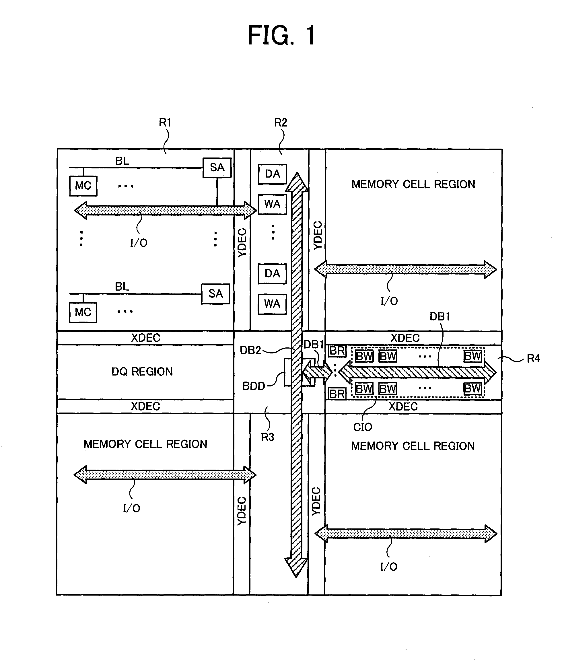
[0033]Preferred embodiments will be described in detail below with reference to accompanying drawings. The following embodiments disclose a DRAM (Dynamic Random Access Memory) as an example of the semiconductor device.

[0034]FIG. 1 is a block diagram showing an entire configuration of the DRAM of the embodiments. The DRAM shown in FIG. 1 is partitioned into a memory cell region R1, an amplifier region R2, a center region R3, and a DQ region R4. In the memory cell region R1, there are provided a plurality of memory cells MC arranged at intersections of a plurality of word lines (not shown) and a plurality of bit lines BL, a plurality of sense amplifiers SA connected to one ends of the bit lines BL, and a plurality of input / output lines I / O selectively connected to the sense amplifiers SA. In addition, an X decoder XDEC arranged at an end in a word line extending direction and a Y decoder YDEC arranged at an end in a bit line extending direction are attached to the memory cell region R...


PUM


Abstract

A semiconductor device is disclosed which comprises a first wiring layer, a second wiring layer formed over the first wiring layer, data input / output terminals, and a data bus formed in the first and second wiring layers. The data bus includes N data lines transmitting data between a predetermined circuit and the input / output terminals. M first data lines among the N data lines have a length shorter than a predetermined length and residual N-M second data lines have a length longer than the predetermined length. Shield lines adjacent to the N data lines are formed in the first and second layers. The N data lines are arranged at positions at which the data lines do not overlap one another in a stacking direction of the first and second wiring layers.

Description

BACKGROUND OF THE INVENTION[0001]1. Field of the Invention[0002]The present invention relates to a semiconductor device comprising a data bus including data lines transmitting data, and a plurality of data input / output terminals for inputting / outputting transmission data of the data bus from / to outside.[0003]2. Description of Related Art[0004]In recent years, increases in capacity and speed have been achieved in semiconductor devices such as DRAM (Dynamic Random Access Memory) that are capable of storing data in a plurality of memory cells, and thus a configuration is required in which transmission data can be transferred with high speed from / to outside through a data bus arranged in a high density. For example, assuming a configuration shown in later-described FIGS. 1 to 4 as a general configuration of the DRAM, data read out from a memory cell is transmitted to a data bus DB1 through an internal circuit, and is transmitted from the data bus DB1 to DQ pads in synchronization with a...

Claims


Application Information

Patent Timeline
Patent Type & Authority Patents(United States)
IPC IPC(8): G11C7/02
CPCH01L23/5222H01L27/10897G11C5/063H01L23/5225H01L27/0207H01L2924/0002G11C7/02G11C11/4097H10B12/50H01L2924/00
Inventor ONDA, TAKAMITSUNAGAMINE, HISAYUKI
Owner LONGITUDE LICENSING LTD
Why Eureka
Try Eureka