Asymmetric slotted waveguide and method for fabricating the same

a technology of slotted waveguides and waveguides, which is applied in the field of slotted waveguides, can solve the problems of increasing the amount of contaminants in the waveguide structure, slow and fast fabrication methods of strip loaded waveguides, and difficulty in achieving the desired high accuracy, etc., and achieves enhanced coupling and shrinking the critical dimension of the features of printed wafers.

Active Publication Date: 2014-03-04
BAE SYST INFORMATION & ELECTRONICS SYST INTEGRATION INC
View PDF6 Cites 2 Cited by
  • Summary
  • Abstract
  • Description
  • Claims
  • Application Information

AI Technical Summary

Benefits of technology

[0013]A standard photolithographic process (e.g., a standard 248 nm DUV photolithographic process) can be adapted to coat the photo resist material on the wafers. An additional shrinking process can be performed to shrink the critical dimension of the features of the printed wafer. The anti-reflective coating (TARC) applied on the wafers can be such as, for example, an AZ Electronics Aquatar VII at a thickness of 430 A. The anti-reflective coating can be an aqueous material that is removed from the wafers during the puddle develop process. The coat / develop portion of the puddle develop process can be performed on a FSI Polaris 2500 Lithography cluster. The wafers can be baked on a proximity bake plate such as for example, the post exposure bake (PEB) is performed on FSI's Transient Thermal Unit (TTU) hot plate with a lid temperature of 120 C. A Polaris 2500 cluster is utilized to shrink the wafers by applying 2000 A of TOK FC-5010 SAFIER as a shrink agent. The SAFIER chemistry can effectively full features such as, vies and slots by shrinking the critical dimension (CD) of the printed slot wafers. The wafers can be processed with the baking process twice in order achieve the desired critical dimension.
[0014]The asymmetric strip-loaded slot waveguides described herein can be utilized for the suppression of the second order TE optical mode or TE1 optical mode. The asymmetric strip-loaded slot waveguides can be also employed for achieving an enhanced coupling with a curved coupler from a ridge waveguide. The fabrication method disclosed herein may not be limited to fabricate the asymmetric slotted waveguides; the proposed method can be alternatively employed to fabricate the symmetric slotted waveguides. The fabrication method for the symmetric slotted waveguides requires a separate step for slot etching. The asymmetric waveguide and method of fabrication described herein therefore permits the slots to be shrunk through a wide range of processes (such as SAFIER or use of side all spacers) to the sub-lithographic dimensions.

Problems solved by technology

At higher frequencies where the span of the waveguide cross section is physically small, it has been difficult to achieve the desired high accuracies.
Most of the prior art methods for fabricating the strip loaded waveguide are very slow and impractical for growing waveguide structures that are compatible for a wide range of electro-optic modulations.
Further, the prior art processes may increase the amount of contaminants in the waveguide structure.
Such contaminants may also contribute to optical losses in the waveguide structure.

Method used


Image

  • Asymmetric slotted waveguide and method for fabricating the same
  • Asymmetric slotted waveguide and method for fabricating the same
  • Asymmetric slotted waveguide and method for fabricating the same

Examples


Embodiment Construction

[0018]The particular values and configurations discussed in these non-limiting examples can be varied and are cited merely to illustrate at least one embodiment and are not intended to limit the scope thereof.

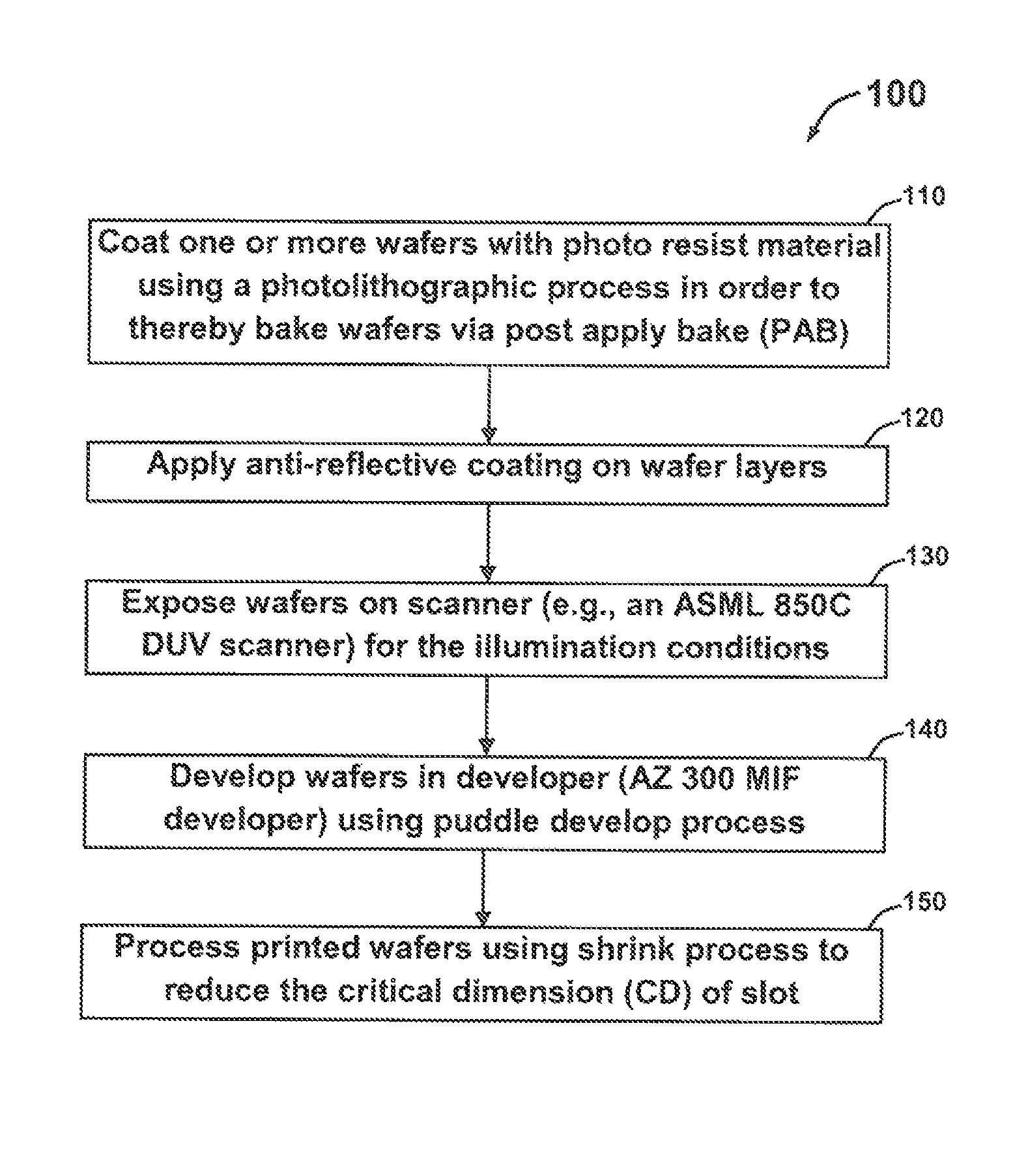
[0019]FIG. 1 illustrates a high level flowchart of operation illustrating logical operational steps of a method for fabricating an asymmetric slotted waveguide, in accordance with the disclosed embodiments. The slotted waveguide is constructed in silicon-on-insulator using a Complementary metal-oxide-semiconductor (CMOS) process. Silicon-on-Insulator Resonators comprising high-Q micro rings were fabricated from thin silicon-on-insulator (SOI) layers. Measured Q values of 45 000 were observed in these rings, which were then improved to 57 000 by adding a PMMA cladding. Various waveguide designs were calculated, and the waveguide losses were analyzed. It is recognized that several forms of silicon on insulator, such as SOI comprising wafers having a silicon oxide layer fabricated...


PUM

PropertyMeasurementUnit
critical dimensionaaaaaaaaaa
semiconductoraaaaaaaaaa
thicknessaaaaaaaaaa

Abstract

An asymmetric slotted waveguide and method for fabricating the same. The slotted waveguide is constructed in silicon-on-insulator using a Complementary metal-oxide-semiconductor (CMOS) process. One or more wafers can be coated with a photo resist material using a photolithographic process in order to thereby bake the wafers via a post apply bake (PAB) process. An anti-reflective coating (TARC) can be further applied on the wafers and the wafers can be exposed on a scanner for the illumination conditions. After a post exposure bake (PEB), the wafers can be developed in a developer using a puddle develop process. Finally, the printed wafers can be processed using a shrink process to reduce the critical dimension (CD) of the slot and thereby achieve an enhanced asymmetric slotted waveguide that is capable of guiding the optical radiation in a wide range of optical modulation applications using an electro-optic polymer cladding.

Description

CROSS-REFERENCE TO RELATED APPLICATIONS[0001]This Application claims rights under 35 USC §119(e) from U.S. Application Ser. No. 61 / 419,464 filed Dec. 3, 2010, the contents of which are incorporated herein by reference.TECHNICAL FIELD[0002]Embodiments are generally related to slotted measuring waveguides. Embodiments are also related to the complementary metal-oxide-semiconductor (CMOS) process. Embodiments are additionally related to methods for fabricating slotted waveguides using the CMOS process.BACKGROUND OF THE INVENTION[0003]Electra-optic materials such as for example, but not limited to gallium arsenide (GaAs) and lithium niobate (Lib03) are employed in wide range of electronic / photonic processes for processing optical signals. The electro-optic materials can change their optical properties in response to an electrical effect. Such materials are widely incorporated within the electronic devices for use in the telecommunications field in order to perform processing activities ...

Claims


Application Information

Patent Timeline
Patent Type & Authority Patents(United States)
IPC IPC(8): G02B1/11H01L33/00H01L27/12G03F7/20H01L21/302
CPCG02B1/11H01L21/8238H01L27/13
Inventor POMERENE, ANDREW T SREINHARDT, WESLEY D.HILL, CRAIG M.
Owner BAE SYST INFORMATION & ELECTRONICS SYST INTEGRATION INC
Why Eureka
Try Eureka