
Organic semiconductors capable of ambipolar transport

a technology of organic semiconductors and ambipolar transport, which is applied in the direction of transistors, solid-state devices, thermoelectric devices, etc., can solve the problems of poor stability of low work function electrodes and low mobility of materials, and achieve the effect of improving transport and easy integration

Active Publication Date: 2014-04-01
THE TRUSTEES OF THE UNIV OF PENNSYLVANIA
View PDF21 Cites 7 Cited by
  • Summary
  • Abstract
  • Description
  • Claims
  • Application Information

AI Technical Summary

Benefits of technology

The patent text describes a method to modify the electrodes in an organic thin film transistor (OTFT) using organic compounds such as aliphatic and aromatic thiols. This allows the creation of OTFT devices that can transport both holes and electrons (both p- and n-type). Compared to non-modified electrodes, the modified devices show significantly better transport for both n- and p-type transport. The transistor can be operated as either an n-type or p-type semiconductor depending on the polarity of the gate voltage. This approach has advantages for mass-production and cost standpoints and can lead to the fabrication of more complex circuits using a single homogeneous semiconductor layer.

Problems solved by technology

The drawbacks of these structures are (i) the poor stability of the low work function electrodes and (ii) two different metals require multiple angled depositions or lithography / masking steps.
Ambipolar transport has been reported in low bandgap organic semiconductors using Au electrodes, but these materials have low mobility.

Method used


Image

  • Organic semiconductors capable of ambipolar transport
  • Organic semiconductors capable of ambipolar transport
  • Organic semiconductors capable of ambipolar transport

Examples


examples

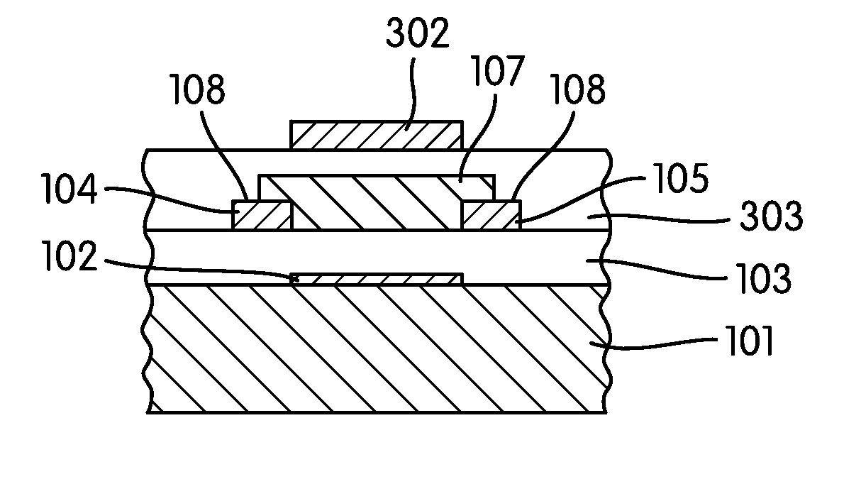
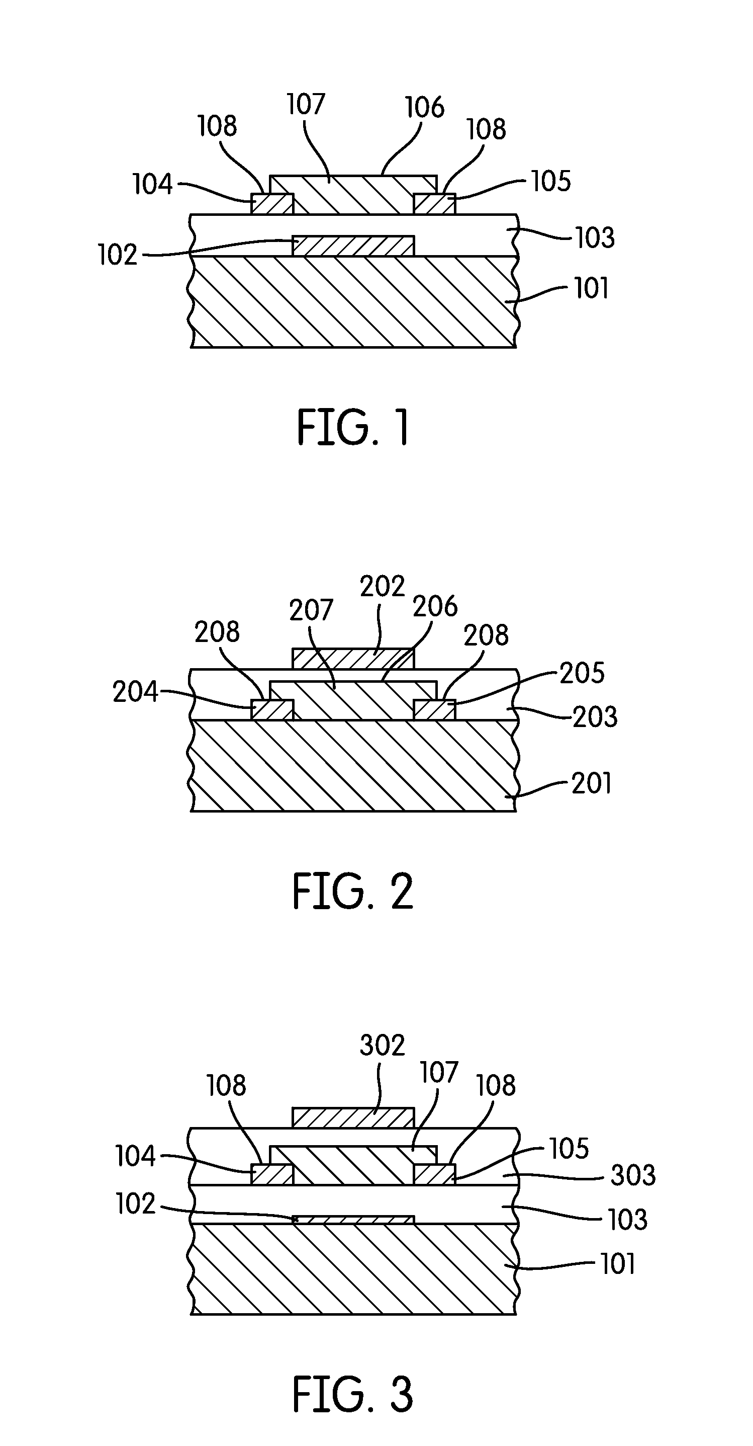
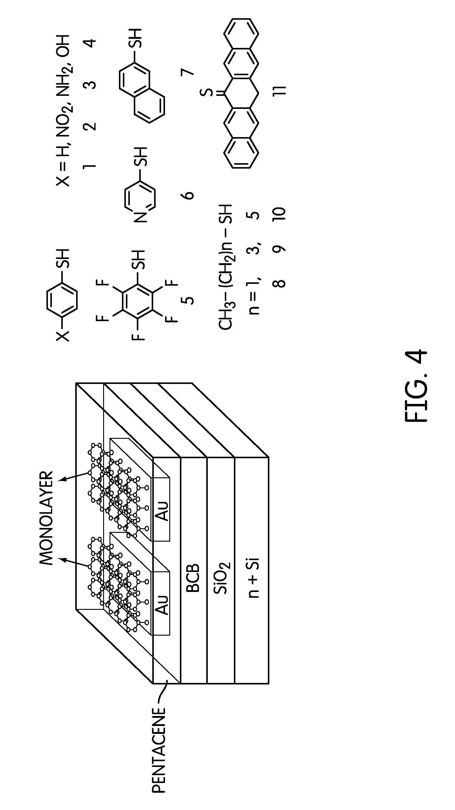
[0038]Pentacene FETs were fabricated in bottom contact geometry, as illustrated in FIG. 4. N-type Si wafers (ρ2 served as the back gate and part of the gate-dielectric stack of the FETs, respectively. The substrates were transferred into a N2-glove box where all the device fabrication and characterization was performed. The wafers were cleaned by UV-ozone for 20 min. A 1:3 solution of BCB:mesitylene was filtered (0.2 μm polytetrafluoroethylene (PTFE) syringe filter), deposited by spin-coating at 3000 rpm for 30 s, and annealed at 265° C. for 30 s, providing a BCB (benzocyclobutene) layer about 130 nm thick. The measured capacitance of the SiO2 (250 nm) / BCB (˜130 nm) gate dielectric stack was 7.6(±0.25) nF / cm2. Au source and drain electrodes (15-20 nm in thickness) were thermally evaporated through a shadow mask to define channel lengths (L) ranging from 30-200 μm and widths (W) to provide W / L of 15 for each device.

[0039]Benzenethiol (1), 4-nitrobenzenethiol (2), 4-aminobenzenethiol ...


PUM


Abstract

Electrodes in an organic thin film transistor based on single component organic semiconductors may be chemically modified to realize ambipolar transport. Electronic circuits may be assembled which include at least two such organic thin film transistors wherein at least one transistor is configured as a pmos transistor and at least on other transistor is configured as a nmos transistor.

Description

CROSS REFERENCE TO RELATED APPLICATIONS[0001]This is a National Phase application of PCT application number PCT / US2009 / 067111, filed Dec. 8, 2009, which claims priority benefit of U.S. provisional application No. 61 / 120,697, filed Dec. 8, 2008, the content of such applications being incorporated herein by reference.FIELD OF THE INVENTION[0002]The invention relates to electronic circuits containing thin film transistors based on organic semiconductors that are capable of realizing ambipolar transport.DISCUSSION OF THE RELATED ART[0003]Ambipolar transport in organic semiconductors has attracted considerable attention for numerous applications of organic complementary metal-oxide semiconductor (CMOS)-like devices in low cost and flexible electronics and in light-emitting and photosensing field-effect transistors (FETs). However, organic semiconductors are commonly classified as either n-type or p-type, as different materials have typically shown unipolar behavior in FETs with, for exam...

Claims


Application Information

Patent Timeline
Patent Type & Authority Patents(United States)
IPC IPC(8): H01L51/00H01L29/786H10K99/00
CPCH01L51/0558H01L51/0545H01L51/0541H01L51/105H01L27/283H10K19/10H10K10/466H10K10/464H10K10/484H10K10/84
Inventor KAGAN, CHERIESAUDARI, SANGAMESHWAR RAO
Owner THE TRUSTEES OF THE UNIV OF PENNSYLVANIA
Learn More