

Coated article
a coating and article technology, applied in the field of coating articles, can solve the problem that the color layer or the housing cannot present metallic appearan
- Summary
- Abstract
- Description
- Claims
- Application Information
AI Technical Summary
Benefits of technology
Problems solved by technology
Method used
Image

Examples
example 1
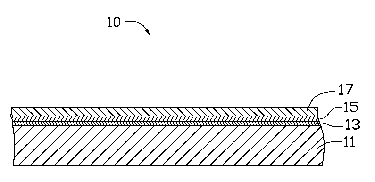
[0018]The substrate 11 was made of stainless steel 315.
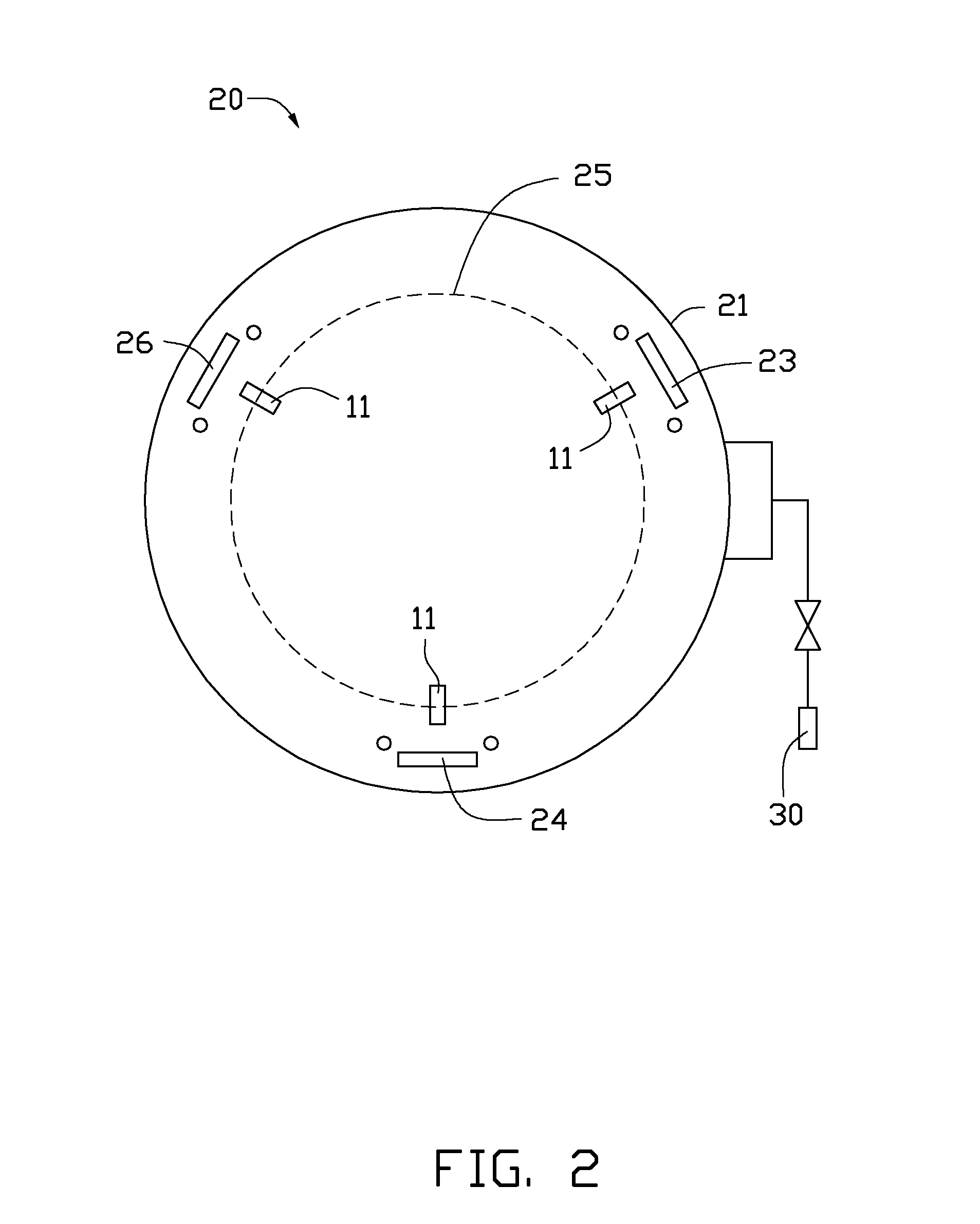
[0019]Sputtering to form the base layer 13 on the substrate 11 took place, wherein the vacuum chamber 21 was heated to a temperature of about 100° C. Ar was fed into the vacuum chamber 21 at a flow rate of about 150 sccm. The chromium target 23 was supplied with a power of about 5 kw. A negative bias voltage of about −250 V was applied to the substrate 11. Deposition of the base layer 13 took a total of about 12 min.
[0020]Sputtering to form the transition layer 15 on the base layer 13 took place, wherein the vacuum chamber 21 was heated to a temperature of about 100° C. Ar was fed into the vacuum chamber 21 at a flow rate of about 125 sccm. Acetylene was fed into the vacuum chamber 21 at a flow rate of about 45 sccm. The chromium target 23 was supplied with a power of about 5 kw. A negative bias voltage of about −250 V was applied to the substrate 11. Deposition of the transition layer 15 took a total of about 40 min.
[0021]Sputt...
example 2
[0023]The substrate 11 was made of aluminum alloy 6061.
[0024]Sputtering to form the base layer 13 on the substrate 11 took place, wherein the vacuum chamber 21 was heated to a temperature of about 90° C. Ar was fed into the vacuum chamber 21 at a flow rate of about 120 sccm. The chromium target 23 was supplied with a power of about 5 kw. A negative bias voltage of about −300 V was applied to the substrate 11. Deposition of the base layer 13 took a total of about 12 min.
[0025]Sputtering to form the transition layer 15 on the base layer 13 took place, wherein the vacuum chamber 21 was heated to a temperature of about 90° C. Ar was fed into the vacuum chamber 21 at a flow rate of about 120 sccm. Acetylene was fed into the vacuum chamber 21 at a flow rate of about 40 sccm. The chromium target 23 was supplied with a power of about 4 kw. A negative bias voltage of about −270 V was applied to the substrate 11. Deposition of the transition layer 15 took a total of about 35 min.
[0026]Sputter...
example 3
[0028]The substrate 11 was made of stainless steel 314.
[0029]Sputtering to form the base layer 13 on the substrate 11 took place, wherein the vacuum chamber 21 was heated to a temperature of about 120° C. Ar was fed into the vacuum chamber 21 at a flow rate of about 135 sccm. The chromium target 23 was supplied with a power of about 6 kw. A negative bias voltage of about −350 V was applied to the substrate 11. Deposition of the base layer 13 took a total of about 15 min.
[0030]Sputtering to form the transition layer 15 on the base layer 13 took place, wherein the vacuum chamber 21 was heated to a temperature of about 105° C. Ar was fed into the vacuum chamber 21 at a flow rate of about 130 sccm. Acetylene was fed into the vacuum chamber 21 at a flow rate of about 50 sccm. The chromium target 23 was supplied with a power of about 6 kw. A negative bias voltage of about −250 V was applied to the substrate 11. Deposition of the transition layer 15 took a total of about 35 min.
[0031]Sputt...
PUM
| Property | Measurement | Unit |
|---|---|---|
| thickness | aaaaa | aaaaa |
| thickness | aaaaa | aaaaa |
| thickness | aaaaa | aaaaa |
Abstract
Description
Claims
Application Information