Active gate drive circuit

a gate drive and active technology, applied in the field of gate drivers, can solve the problems of increased delays and gate driving losses, large switching losses, and small controllability of voltage slop

Active Publication Date: 2014-04-29
ABB (SCHWEIZ) AG
View PDF6 Cites 10 Cited by
  • Summary
  • Abstract
  • Description
  • Claims
  • Application Information

AI Technical Summary

Benefits of technology

[0008]Further possibilities to influence the gate current during the switching transients are for example switchable or adjustable gate resistor(s), current sources / sinks or gate voltages. As the implementation of such gate drives with adjustable output stage has to ensure an operation in the SOA, e.g. limited diC / dt and dvCE / dt, for all operating conditions (varied Tj, iC, vCE), for most of the operating points the desired optimal current and voltage slopes are not achieved leading to increased switching losses. In addition, the system state of the semiconductor, e.g. the transition from the current to the voltage transients and vice versa, should be detected most accurately in an additional complex circuit, to be able to independently adjust diC / dt and dvCE / dt.
[0025]In accordance with exemplary embodiments of the present disclosure the change rate of collector current and the change rate of collector-to-emitter voltage can be controlled using a simple structure. The controlled change rates ensure that problems relating to high change rates or excessive losses are dealt with.

Problems solved by technology

Minimizing switching losses of the IGBT, sticking the current and voltage conditions to the save operating area (SOA), e.g. limiting the turn-off overvoltage and the peak reverse recovery current during turn-on, and restricting electromagnetic interference (EMI) can be a challenging task of the IGBT's gate drive.
This approach can lead either to excessive switching losses or to increased delays and gate driving losses due to the larger amount of gate charge that is specified.
However, in this approach the controllability of the voltage slope is small.
As the implementation of such gate drives with adjustable output stage has to ensure an operation in the SOA, e.g. limited diC / dt and dvCE / dt, for all operating conditions (varied Tj, iC, vCE), for most of the operating points the desired optimal current and voltage slopes are not achieved leading to increased switching losses.
Missing compensation of the IGBT's non-linearities and dependencies on the operating point is a further and main drawback of all these open-loop control topologies.
Due to the implementation with a large amount of bipolar transistors and an active detection and selection of the control loop, the performance was limited to 200 A / μs and 1 kV / μs.

Method used


Image

  • Active gate drive circuit
  • Active gate drive circuit
  • Active gate drive circuit

Examples


Embodiment Construction

[0022]Exemplary embodiments of the present disclosure provide a driving method and driver circuit implementing the method so as to alleviate the above mentioned disadvantages.

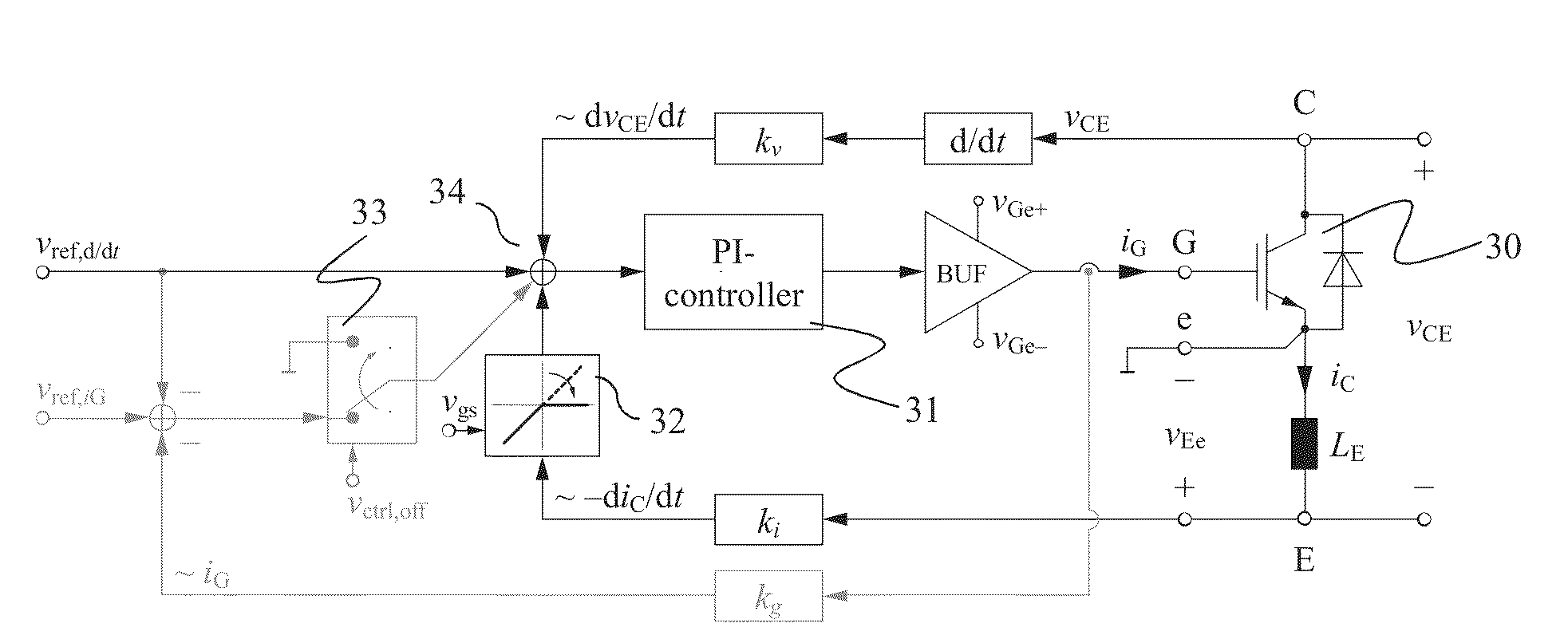
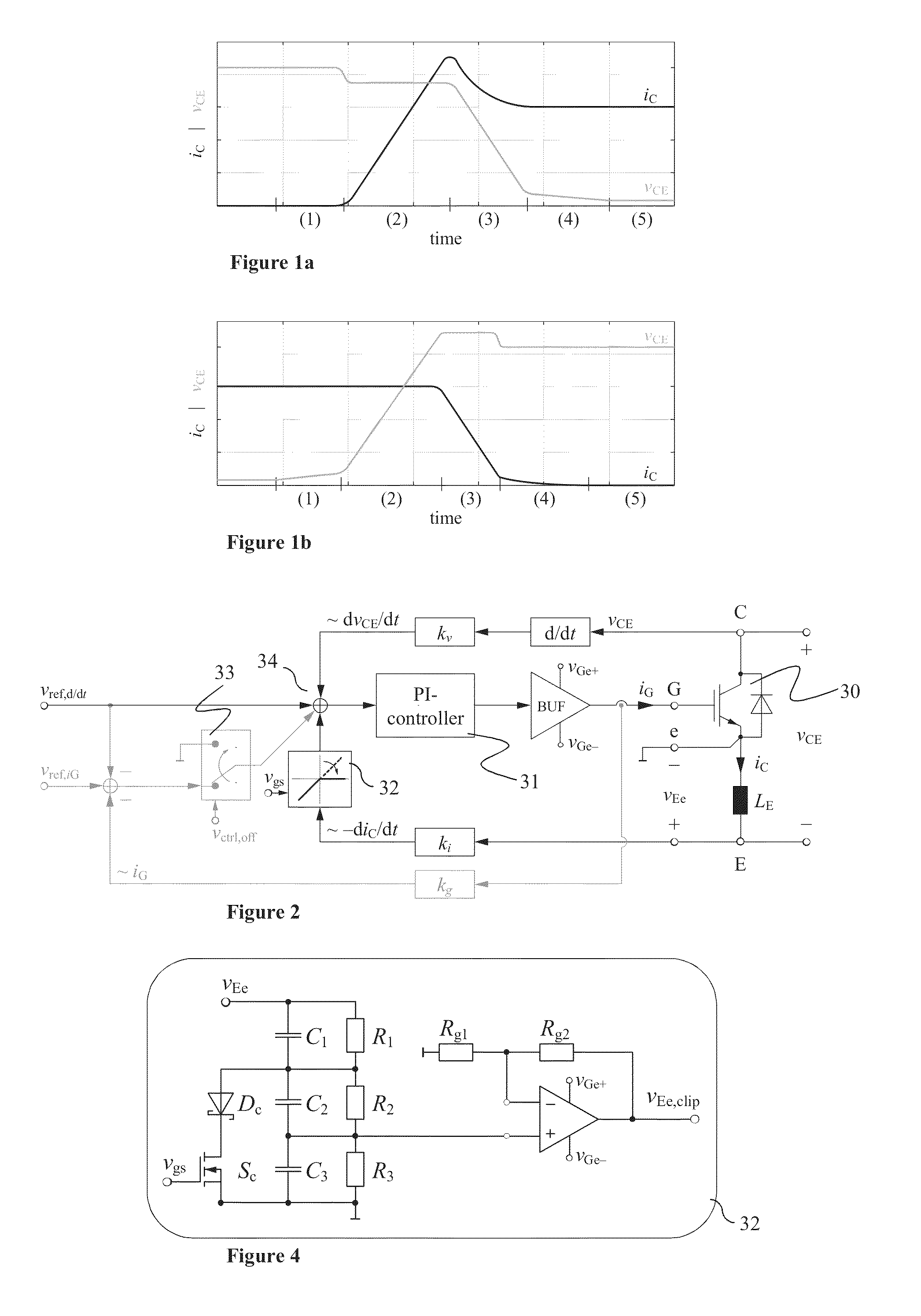
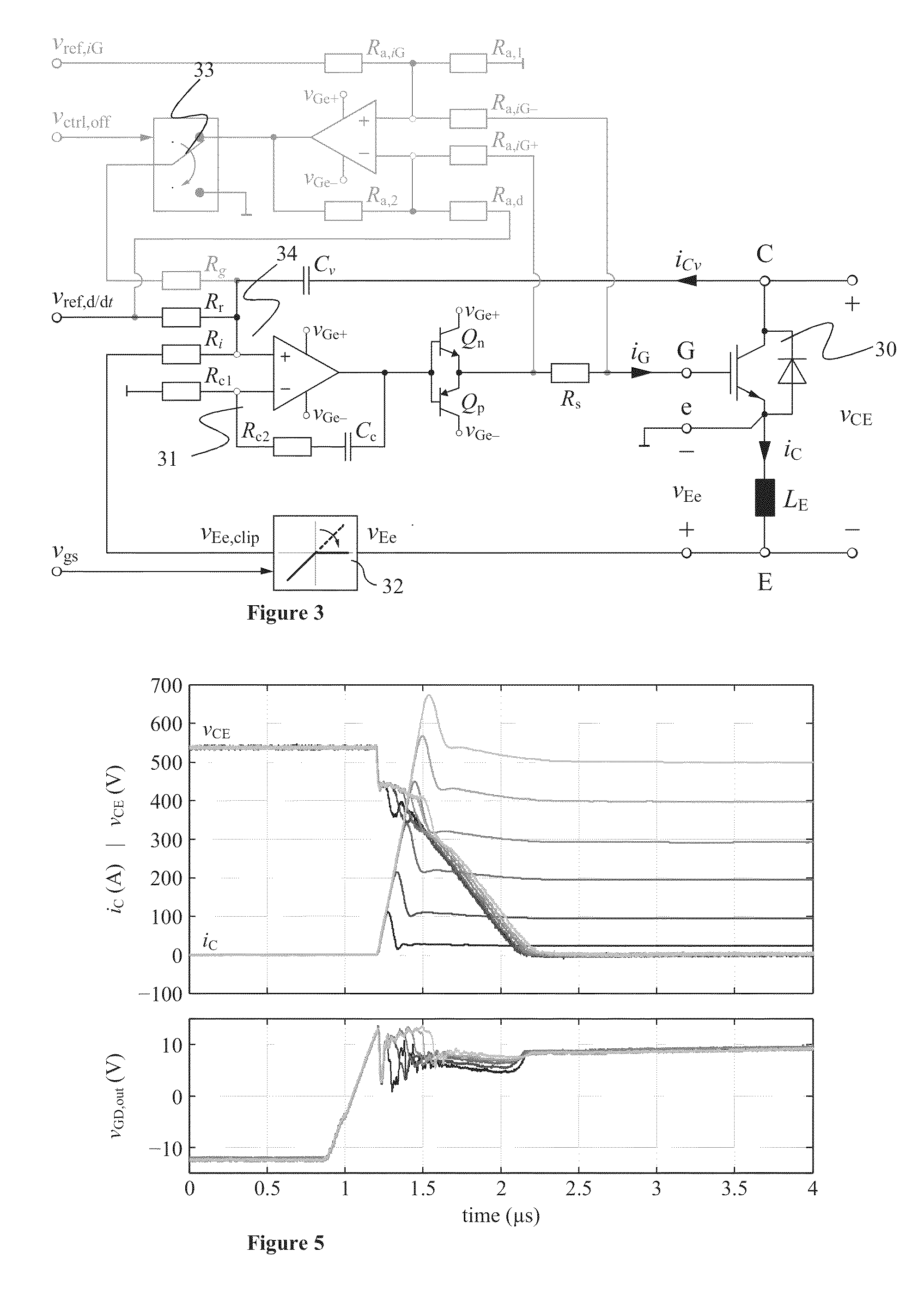
[0023]Exemplary embodiments are based on the idea of using a single PI controller that controls both diC / dt and dvCE / dt of the gate-controlled component. Due to the nature of turn-on and turn-off procedures, either the collector current or the collector-to-emitter voltage changes at a time thereby enabling the use of only one PI controller.

[0024]The active gate drive of exemplary embodiments descried herein provide highly dynamic control using simple hardware implementation. For the hardware implementation only simple measurement circuits, a constant reference signal during the complete switching operation and one single control amplifier can be specified. Due to the natural state transition from diC / dt to dvCE / dt control and vice versa, no active change of the control loop is needed during the switching transi...


PUM


Abstract

Exemplary embodiments are directed to a gate drive circuit and a method for controlling a gate-controlled component. The gate drive circuit includes a PI controller that receives an input reference signal (vref,d / dt) controls a gate voltage of the gate-controlled component. The gate drive circuit also includes a first feedback loop for the PI controller adapted to provide feedback from a time derivative of a collector-to-emitter voltage (vCE) of the controlled component. The first feedback loop has a first gain (kv). A second is provided in the gate drive circuit feedback loop for the PI controller that provides feedback from the time derivative of the collector current (iC) of the controlled component. The second feedback loop has second gain (ki) and includes a clipping circuit that modifies the feedback signal in the second feedback loop during turn-on of the controlled component when the time derivative of the collector current is negative.

Description

RELATED APPLICATION(S)[0001]This application claims priority under 35 U.S.C. §119 to European Patent Application No. 12151032.5 filed in Europe on Jan. 13, 2012, the entire content of which is hereby incorporated by reference in its entirety.FIELD[0002]The present disclosure relates to gate drivers, and to gate drivers employing closed control loop of current and voltage slope.BACKGROUND INFORMATION[0003]Insulated gate bipolar transistor (IGBT) modules are widely used in inductive (hard) switching voltage source power electronic converters such as drives, switched-mode power supplies or solid state transformers.[0004]Minimizing switching losses of the IGBT, sticking the current and voltage conditions to the save operating area (SOA), e.g. limiting the turn-off overvoltage and the peak reverse recovery current during turn-on, and restricting electromagnetic interference (EMI) can be a challenging task of the IGBT's gate drive. Setting the collector current slope diC / dt at turn-on can...

Claims


Application Information

Patent Timeline
Patent Type & Authority Patents(United States)
IPC IPC(8): H03B1/00
CPCH03K17/06H03K17/166H03K17/0828H03K17/08148H03K17/168
Inventor LOBSIGER, YANICHKOLAR, JOHANN WALTERLAITINEN, MATTI
Owner ABB (SCHWEIZ) AG
Why Eureka
Try Eureka