Method of detecting impinging position of photons on a geiger-mode avalanche photodiode, related geiger-mode avalanche photodiode and fabrication process

a technology of avalanche photodiodes and photodiodes, which is applied in the field of photon detection, can solve the problems of difficult application to low-end products, difficult to use wire bonding for packaging, and difficult to integrate detectors with electronics. , to achieve the effect of reducing cross-talk

Active Publication Date: 2014-05-13
STMICROELECTRONICS SRL
View PDF17 Cites 6 Cited by
  • Summary
  • Abstract
  • Description
  • Claims
  • Application Information

AI Technical Summary

Benefits of technology

[0018]According to an embodiment, the metal structure of each photodiode may surround either the resistive anode or the resistive cathode regions of the photodiode and effectively acts also as a metal shield that reduces cross-talk. Another aspect is directed to a fabrication process of the disclosed avalanche photodiode and two different methods of sensing spikes of each photodiode of the array are also disclosed.

Problems solved by technology

The packaging of these devices and the integration of the detector with the electronics is a quite complex matter and various techniques have been developed in recent years to realize compact and cheap “packaging” approaches.
It may be necessary to connect each pixel in the array to appropriate external circuitry such that for arrays with a high number of pixels it may be practically impossible to use the wire bonding for the packaging.
However the high complexity of technology and large amount of cost used for their development made them difficult to apply to low-end products [3].
Unfortunately, Geiger-mode avalanche photodiodes may need relatively complex read circuitry.
The used CMOS technology introduces some limits to device applications: approach complexity; and at least two circuits may be needed, one to bias the device and one to read an output signal.
This may increase device fabrication costs, in particular due to the readout system manufacture, and may reduce in a significant way the ratio between the sensitivity area and the overall area (geometrical fill factor), affecting as a consequence array sensitivity.
CMOS technology is not optimized for high sensitivity detectors and has noise problems such as dark counts, afterpulsing and so on [6].

Method used


Image

  • Method of detecting impinging position of photons on a geiger-mode avalanche photodiode, related geiger-mode avalanche photodiode and fabrication process
  • Method of detecting impinging position of photons on a geiger-mode avalanche photodiode, related geiger-mode avalanche photodiode and fabrication process
  • Method of detecting impinging position of photons on a geiger-mode avalanche photodiode, related geiger-mode avalanche photodiode and fabrication process

Examples


Embodiment Construction

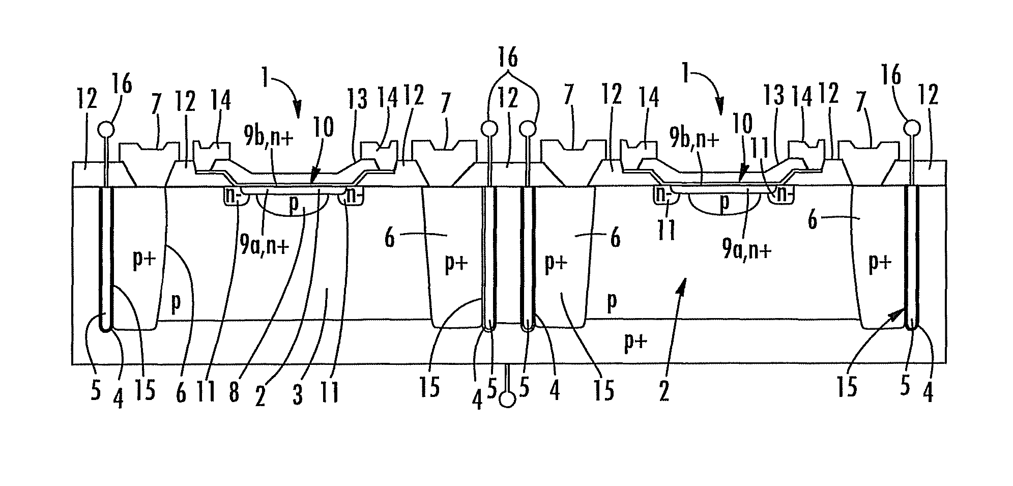
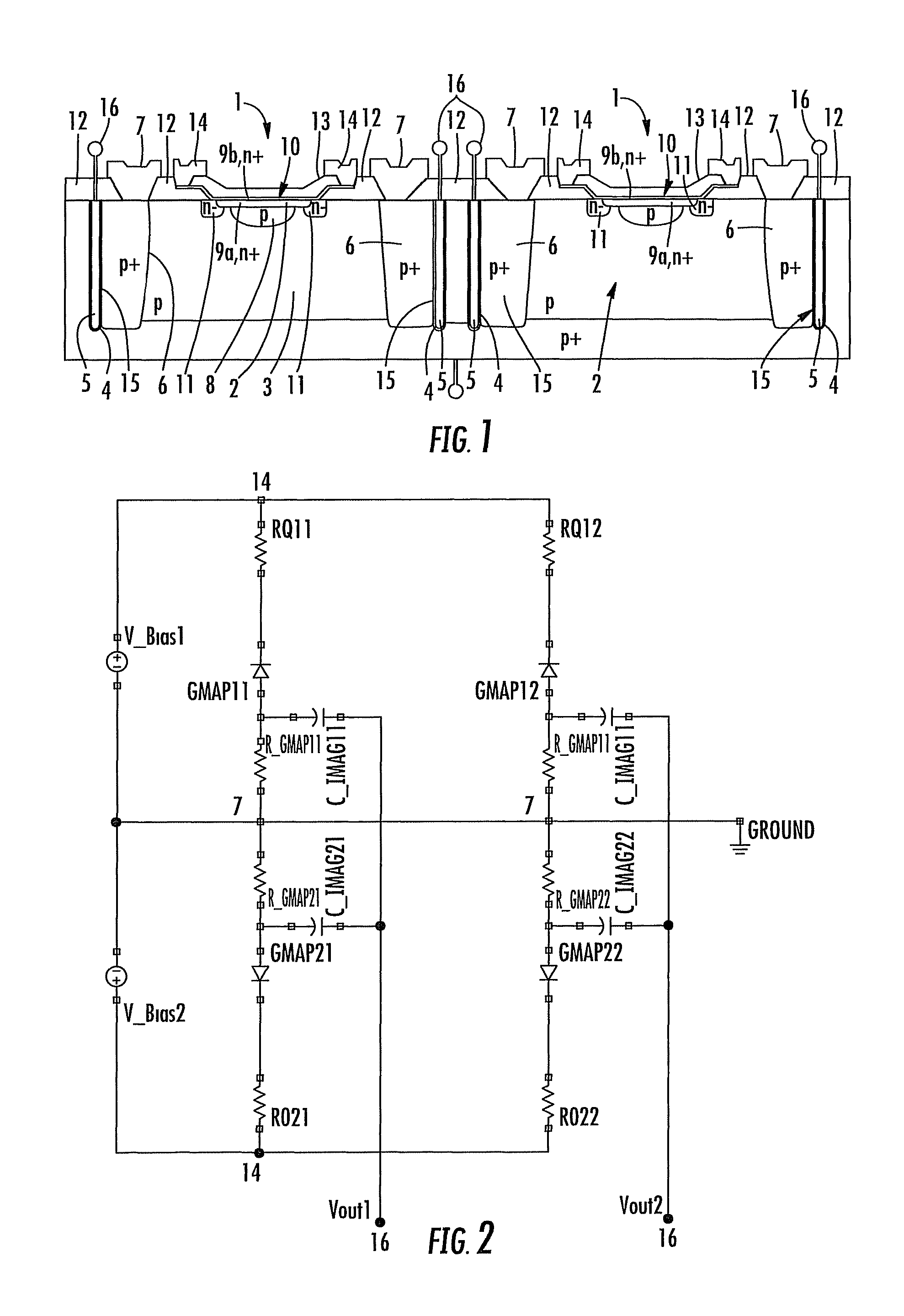
[0026]A exemplary structure of an array of Geiger-mode avalanche photodiodes is schematically illustrated in FIG. 1. In the depicted example, only two photodiodes are shown, though the array may comprise any number of photodiodes organized in rows and columns. The avalanche photodiode has three terminals instead of two: a cathode contact 14, an anode contact 7, a metal structure 5 having a terminal 16 on which spikes correlated to avalanche events of the photodiode may be sensed. The metal structure 5 is defined in a trench coated with a dielectric 4, preferably silicon oxide, and is thus capacitively coupled with a region of the photodiode, that in the shown example is the anode diffusion 6.

[0027]Other details of the embodiment of FIG. 1, such as the definition of the cathode and anode regions and the definition of the metal structures, may be discussed later. The avalanche photodiode has anode or cathode diffusion that opposes a resistance (even if it may be relatively small) to a...


PUM


Abstract

A Geiger-mode avalanche photodiode may include an anode, a cathode, an output pad electrically insulated from the anode and the cathode, a semiconductor layer having resistive anode and cathode regions, and a metal structure in the semiconductor layer and capacitively coupled to a region from the resistive anode and resistive cathode regions and connected to the output pad. The output pad is for detecting spikes correlated to avalanche events.

Description

FIELD OF THE INVENTION[0001]The preset invention is generally directed to the field of photon detection, and in particular, the detection of individual photons. In particular, the present invention refers to position sensitive monolithic arrays of Geiger-Mode Avalanche Photodiodes (GMAPs) and to related integrated readout systems.BACKGROUND OF THE INVENTION[0002]Detector arrays are used in a wide variety of imaging systems for industrial as well as scientific applications. For example, detector arrays have been recently widely used in nuclear medical imaging techniques such as Positron Emission Tomography (PET). In this application, 511 keV gamma rays, emitted by the human body, strike pixelated scintillators which create light in response to the received radiation. Each illuminated pixel of the pixelated scintillator is detected in the detector array by a respective photodiode, which converts the light into electrical signals used for imaging purposes. During data collection, each ...

Claims


Application Information

Patent Timeline
Patent Type & Authority Patents(United States)
IPC IPC(8): H01L31/107H01L31/18H01L27/146
CPCH01L27/1446H01L27/14689H01L31/107H01L31/022408
Inventor SANFILIPPO, DELFO NUNZIATOCONDORELLI, GIOVANNI
Owner STMICROELECTRONICS SRL
Why Eureka
Try Eureka