
Light harvesting system employing microstructures for efficient light trapping

a microstructure and light trapping technology, applied in the field of light trapping system employing microstructures for efficient light trapping, can solve the problems of poor light absorption of long wavelength light, high cost of this thick layer of silicon, and high cost of devices, and achieve the effect of substantially enhancing the effect of light absorption

Active Publication Date: 2014-05-27
S V V TECH INNOVATIONS
View PDF12 Cites 4 Cited by
  • Summary
  • Abstract
  • Description
  • Claims
  • Application Information

AI Technical Summary

Benefits of technology

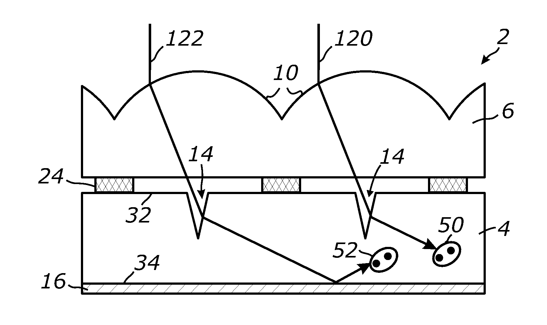
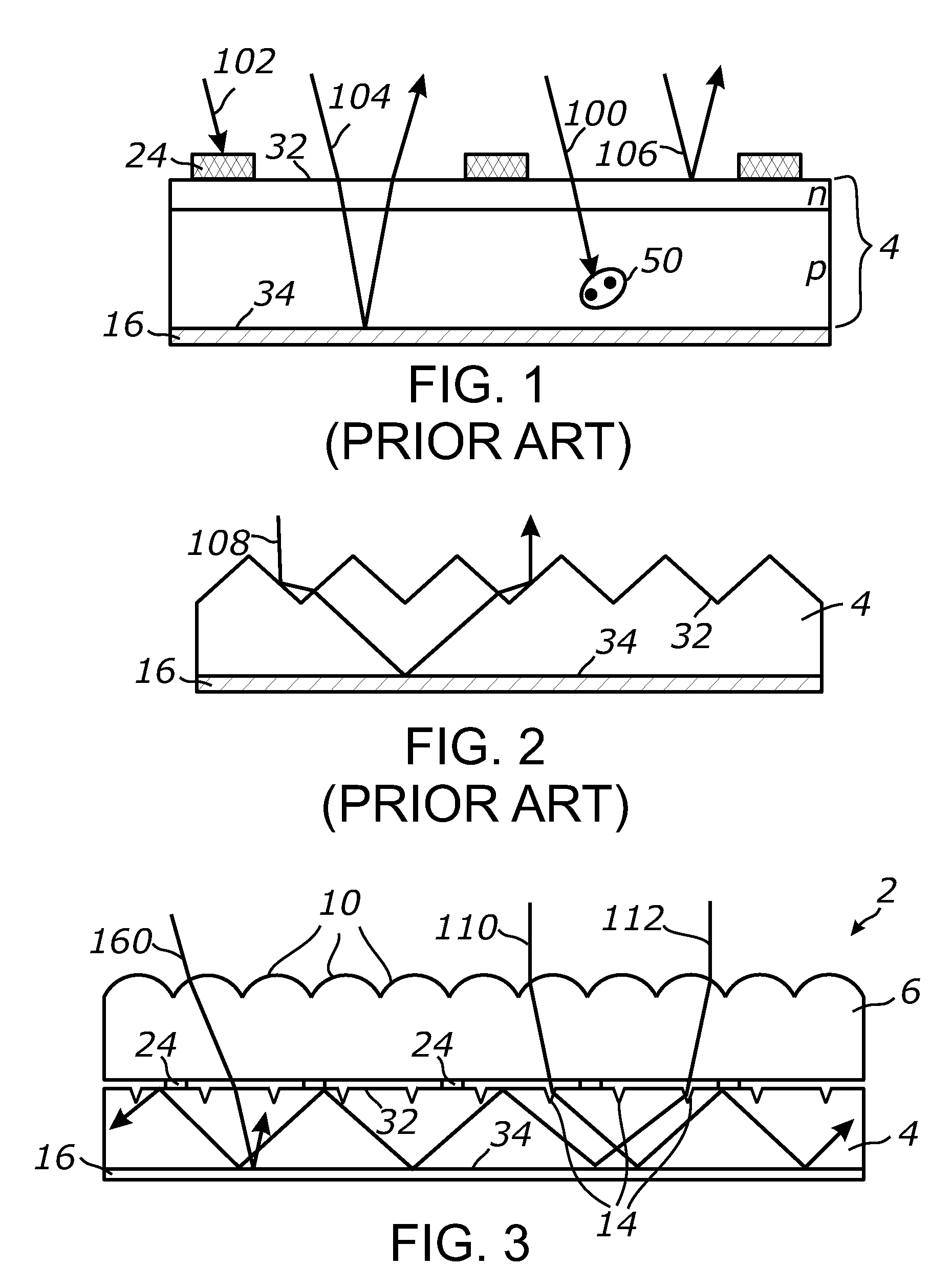
[0015]The present invention solves a number of light harvesting problems within a compact system utilizing efficient light coupling and trapping mechanisms. Light is injected into a photoresponsive layer through light input ports using a focusing array and trapped within the layer so that the useful light absorption is substantially enhanced.
[0027]An element of the invention is a light harvesting system collecting light over a given area and communicating the incident light into a photoresponsive layer, such as a photovoltaic layer, with an enhanced light coupling efficiency and with increasing the light path through the photoresponsive layer.
[0030]Another element of the invention is the inclusion of one or more cladding layers or mirrored surfaces to enhance respectively the total internal reflection or the specular reflection of light within the photoresponsive layer.
[0031]Another element of the invention is the use of electrical contacts which can additionally be provided with enhanced reflective properties to promote retaining the light within the photoresponsive layer.

Problems solved by technology

However, Si is an indirect bandgap semiconductor and is poorly absorbing the long wavelength light.
While Si is very abundant, stable and well-suited for solar cell and light detector manufacturing, the cost of this thick layer of silicon is quite high which results in the high cost of the devices.
However, the existing approaches for light trapping in the photovoltaic devices cannot prevent for a substantial portion of incident light to escape from the device without being absorbed.
For example, in case of the front surface employing random pyramidal microstructures, a large portion of the escaping light is usually lost through this front surface due to the random nature of the secondary interactions of the light rays with the pyramids.
Furthermore, up to 10 percent or more light can be lost in conventional photovoltaic systems due to the reflection from front contacts or absorption by layers or surfaces which produce no photovoltaic effect.
An additional problem encountered in photovoltaic devices is that most photovoltaic materials have a relatively large refractive index which results in poor light coupling efficiency due to the high reflection losses from the light receiving surface.
However, the antireflective coating works efficiently only in a limited bandwidth and adds system cost and processing time, while the microstructures are still somewhat inefficient for light coupling or otherwise are quite expensive to be used for mass production, considering that the entire area of the photovoltaic device must be processed to cover it with these microstructures.
These drawbacks of the prior art approaches and the loss of useful light are hampering the utility of the photovoltaic devices.
None of the previous efforts provides an efficient solution for coupling and trapping essentially all of the incident light and allowing it to pass through the sufficient effective depth of photosensitive material or allow the light to interact with the active layer as many times as necessary to cause the efficient light absorption in a controlled manner.

Method used


Image

  • Light harvesting system employing microstructures for efficient light trapping
  • Light harvesting system employing microstructures for efficient light trapping
  • Light harvesting system employing microstructures for efficient light trapping

Examples


Embodiment Construction

[0059]Referring more specifically to the drawings, for illustrative purposes the present invention is embodied in the apparatus generally shown in the preceding figures. It will be appreciated that the apparatus may vary as to configuration and as to details of the parts without departing from the basic concepts as disclosed herein. Furthermore, elements represented in one embodiment as taught herein are applicable without limitation to other embodiments taught herein, and in combination with those embodiments and what is known in the art.

[0060]A wide range of applications exist for the present invention in relation to the collection of electromagnetic radiant energy, such as light, in a broad spectrum or any suitable spectral bands or domains. Therefore, for the sake of simplicity of expression, without limiting generality of this invention, the term “light” will be used herein although the general terms “electromagnetic energy”, “electromagnetic radiation”, “radiant energy” or exe...


PUM


Abstract

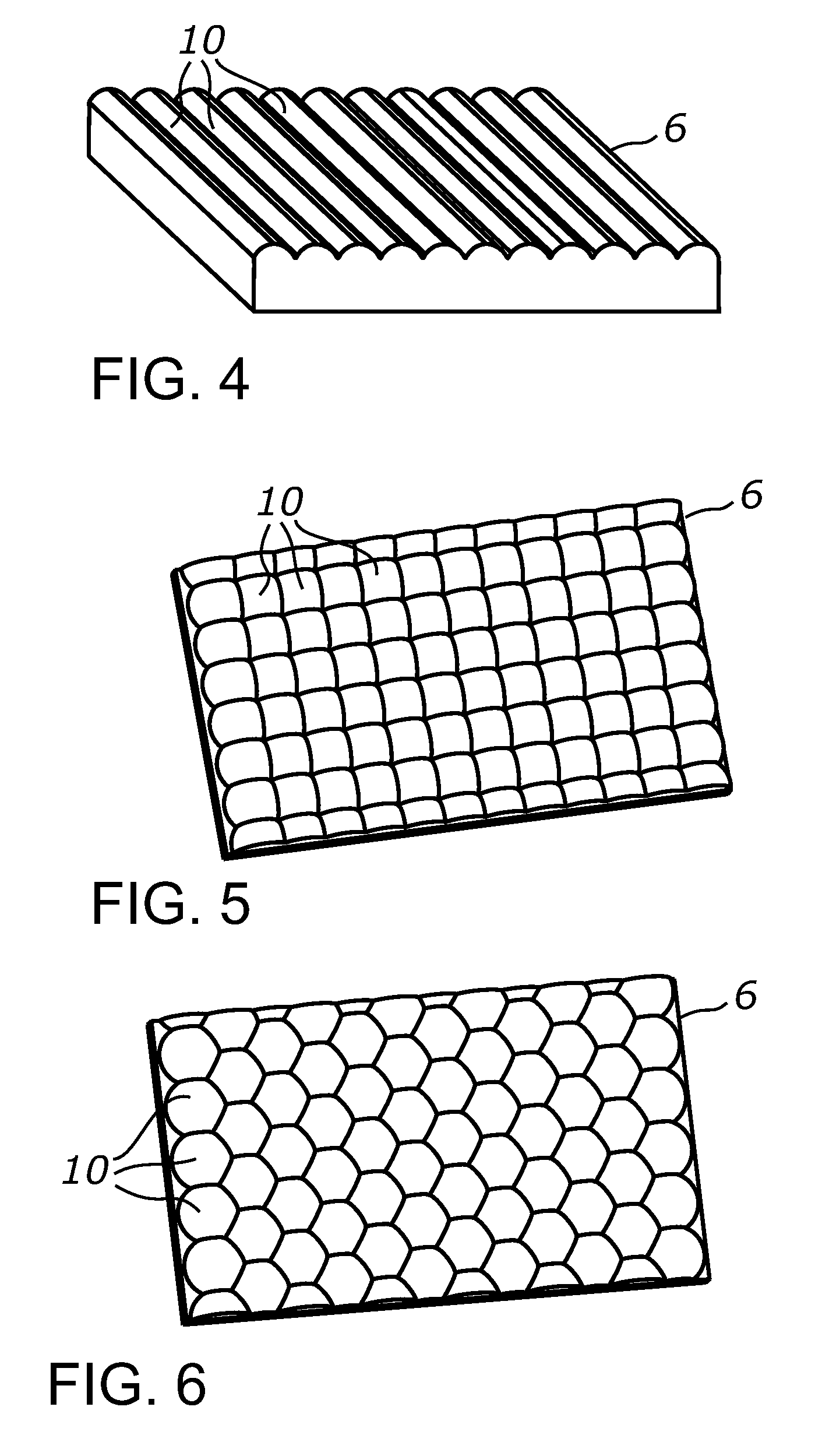
A light harvesting system employing a focusing array and a photoresponsive layer in which a plurality of microstructured areas is formed. Light received by the focusing array is injected transmissively into the photoresponsive layer through the microstructured areas. The injected light is retained in the photoresponsive layer by at least a total internal reflection and is propagated within the layer until it is substantially absorbed.

Description

CROSS-REFERENCE TO RELATED APPLICATIONS[0001]This application claims priority from U.S. provisional application Ser. No. 61 / 399,552 filed on Jul. 13, 2010, incorporated herein by reference in its entirety, and from U.S. provisional application Ser. No. 61 / 402,061 filed on Aug. 21, 2010 incorporated herein by reference in its entirety.STATEMENT REGARDING FEDERALLY SPONSORED RESEARCH OR DEVELOPMENT[0002]Not ApplicableINCORPORATION-BY-REFERENCE OF MATERIAL SUBMITTED ON A COMPACT DISC[0003]Not ApplicableNOTICE OF MATERIAL SUBJECT TO COPYRIGHT PROTECTION[0004]A portion of the material in this patent document is subject to copyright protection under the copyright laws of the United States and of other countries. The owner of the copyright rights has no objection to the facsimile reproduction by anyone of the patent document or the patent disclosure, as it appears in the United States Patent and Trademark Office publicly available file or records, but otherwise reserves all copyright right...

Claims


Application Information

Patent Timeline
Patent Type & Authority Patents(United States)
IPC IPC(8): H01L31/00
CPCH01L31/02327G02B5/0231H01L31/0525G02B5/0294G01J5/0853G01J1/0407Y02E10/52H01L31/0522H01L31/0547H01L31/054H01L31/0543G02B19/0028
Inventor VASYLYEV, SERGIY
Owner S V V TECH INNOVATIONS
Learn More