Optical characterization systems employing compact synchrotron radiation sources

Active Publication Date: 2014-06-10
KLA TENCOR CORP
View PDF7 Cites 29 Cited by
  • Summary
  • Abstract
  • Description
  • Claims
  • Application Information

AI Technical Summary

Benefits of technology

[0010]A synchrotron radiation source for generating light for a semiconductor wafer optical characterization system or a mask optical characterization system is disclosed. In a first aspect, the synchrotron radiation source may include, but is not limited to, an electron beam generator configured to generate one or more beams of electrons; an electron storage ring including a plurality of magnets configured to bend a trajectory of the electrons to trace a closed path; and one or more wiggler insertion devices disposed along at least one straight section of the electron storage ring, the one or more wiggler insertion devices including a plurality of magnetic poles configured to generate a pe

Problems solved by technology

The time-multiplexing of several sources limits inspection throughput, while simultaneously increasing cost and complexity.
In addition, spectral output in DPP and LPP sources cannot be directly controlled in design or operation.
Further, a low cost LPP source suitable for actinic EUV mask inspection can have different spectral properties from a scanner high-power LPP source, thereby increasing the difficulty of relating inspection image information to defect printability.
In addition, pulse repetition rate in LPP and DPP systems is limited by a number of physical constraints, with pulse-pulse energy fluctuations being significant.
Due to the inherent var

Method used


Image

  • Optical characterization systems employing compact synchrotron radiation sources
  • Optical characterization systems employing compact synchrotron radiation sources
  • Optical characterization systems employing compact synchrotron radiation sources

Examples


Embodiment Construction

[0027]It is to be understood that both the foregoing general description and the following detailed description are exemplary and explanatory only and are not necessarily restrictive of the invention as claimed. The accompanying drawings, which are incorporated in and constitute a part of the specification, illustrate embodiments of the invention and together with the general description, serve to explain the principles of the invention. Reference will now be made in detail to the subject matter disclosed, which is illustrated in the accompanying drawings.

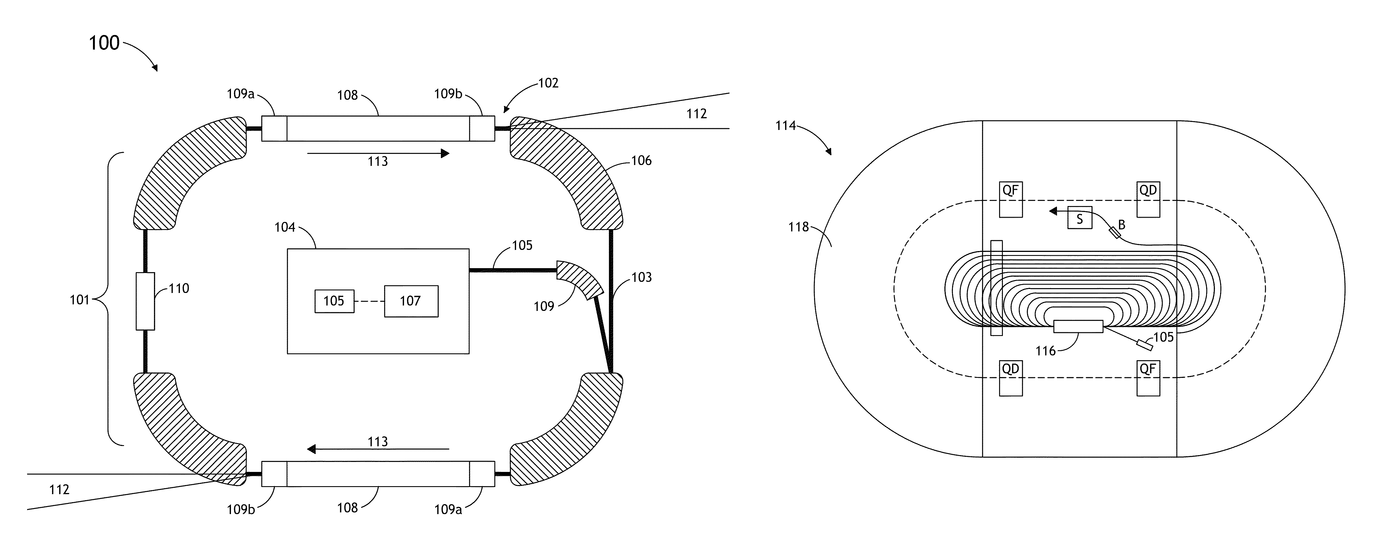
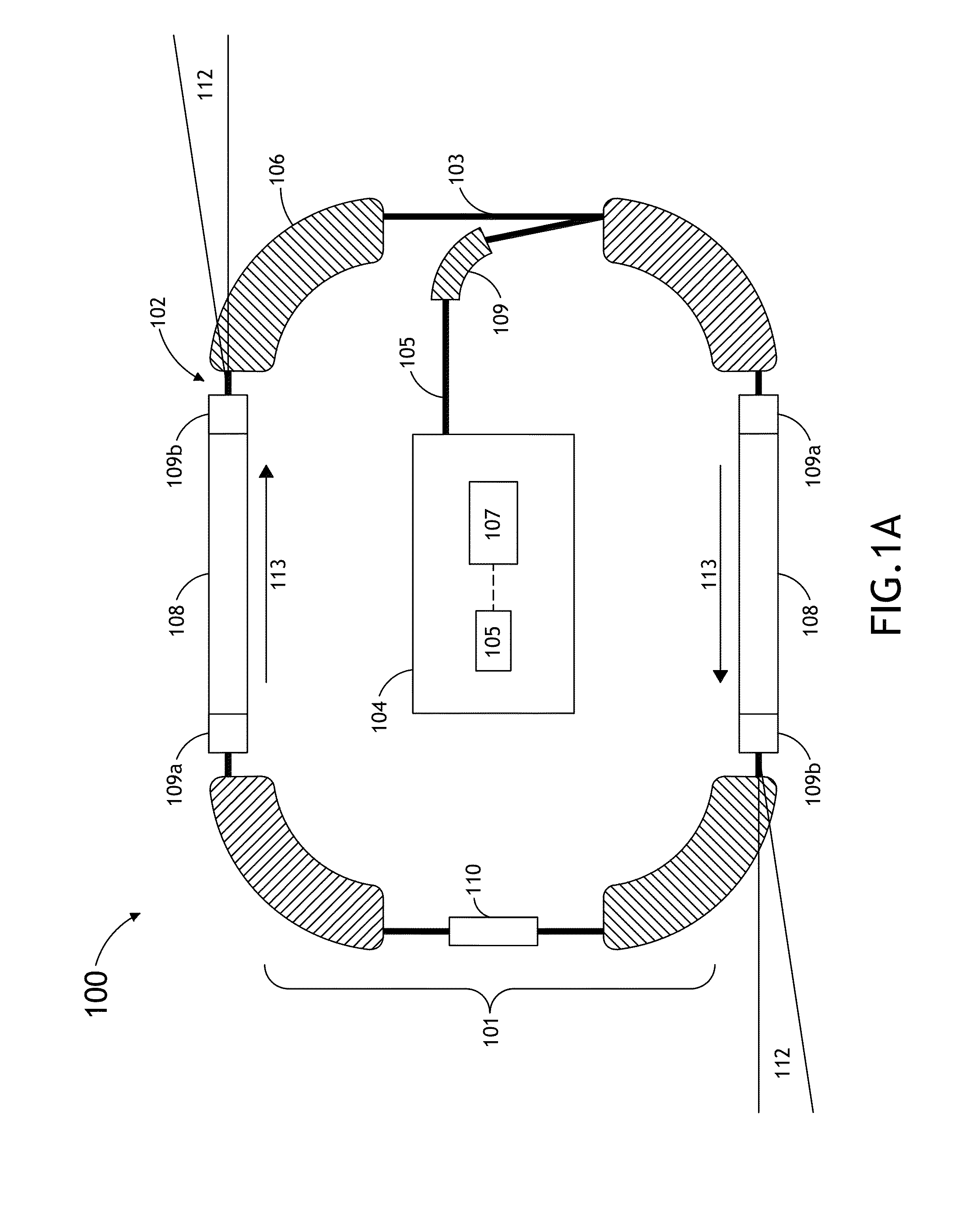
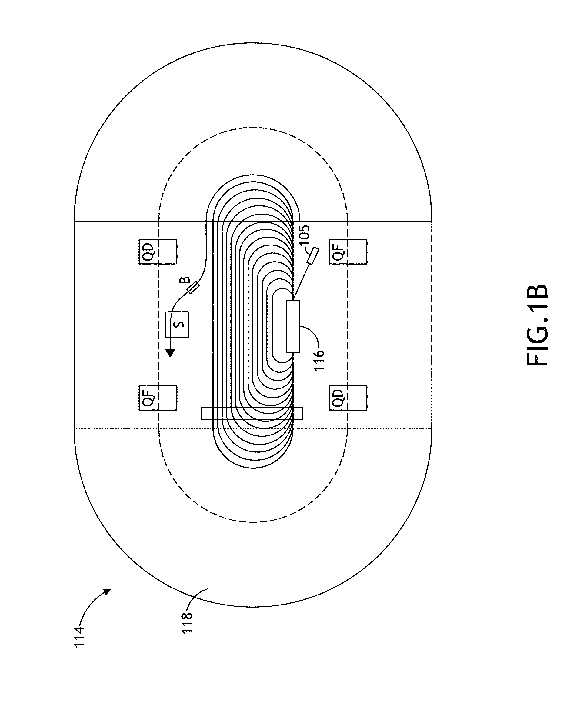
[0028]Referring generally to FIG. 1A through 5, a wiggler based synchrotron radiation source 100 suitable for serving as an illumination source of a semiconductor wafer optical characterization system or a mask optical characterization system is described in accordance with the present invention.

[0029]Synchrotron radiation results from the acceleration of highly relativistic electrons, such as acceleration of electrons in a magnet ...


PUM


Abstract

A compact synchrotron radiation source includes an electron beam generator, an electron storage ring, one or more wiggler insertion devices disposed along one or more straight sections of the electron storage ring, the one or more wiggler insertion devices including a set of magnetic poles configured to generate a periodic alternating magnetic field suitable for producing synchrotron radiation emitted along the direction of travel of the electrons of the storage ring, wherein the one or more wiggler insertion devices are arranged to provide light to a set of illumination optics of a wafer optical characterization system or a mask optical characterization system, wherein the etendue of a light beam emitted by the one or more wiggler insertion devices is matched to the illumination optics of the at least one of a wafer optical characterization system and the mask optical characterization system.

Description

CROSS-REFERENCE TO RELATED APPLICATION[0001]The present application is related to and claims the benefit of the earliest available effective filing date(s) from the following listed application(s) (the “Related Applications”) (e.g., claims earliest available priority dates for other than provisional patent applications or claims benefits under 35 USC §119(e) for provisional patent applications, for any and all parent, grandparent, great-grandparent, etc. applications of the Related Application(s)).RELATED APPLICATIONS[0002]For purposes of the USPTO extra-statutory requirements, the present application constitutes a regular (non-provisional) patent application of United States Provisional Patent Application entitled High Throughput and Availability Wafer and EUV Mask Inspection Systems Employing Low-Cost Wiggler Sources, naming Yanwei Liu and Daniel C. Wack as inventors, filed Aug. 14, 2012, Application Ser. No. 61 / 682,772.TECHNICAL FIELD[0003]The present invention generally relates ...

Claims


Application Information

Patent Timeline
IPC IPC(8): H01J40/00H01J47/00
CPCH05H7/08H05H7/04H01J37/02H05H13/04G21K1/06H05G2/001H05G2/00
Inventor LIU, YANWEIWACK, DANIEL C.
Owner KLA TENCOR CORP
Why Eureka
Try Eureka