Method for fabricating semiconductor device
a technology of semiconductor devices and semiconductor components, applied in the direction of semiconductor devices, basic electric elements, electrical equipment, etc., can solve the problems of face problems, leakage current, conventional polysilicon gate, etc., and achieve the effect of improving bottlenecks
- Summary
- Abstract
- Description
- Claims
- Application Information
AI Technical Summary
Benefits of technology
Problems solved by technology
Method used
Image

Examples
Embodiment Construction
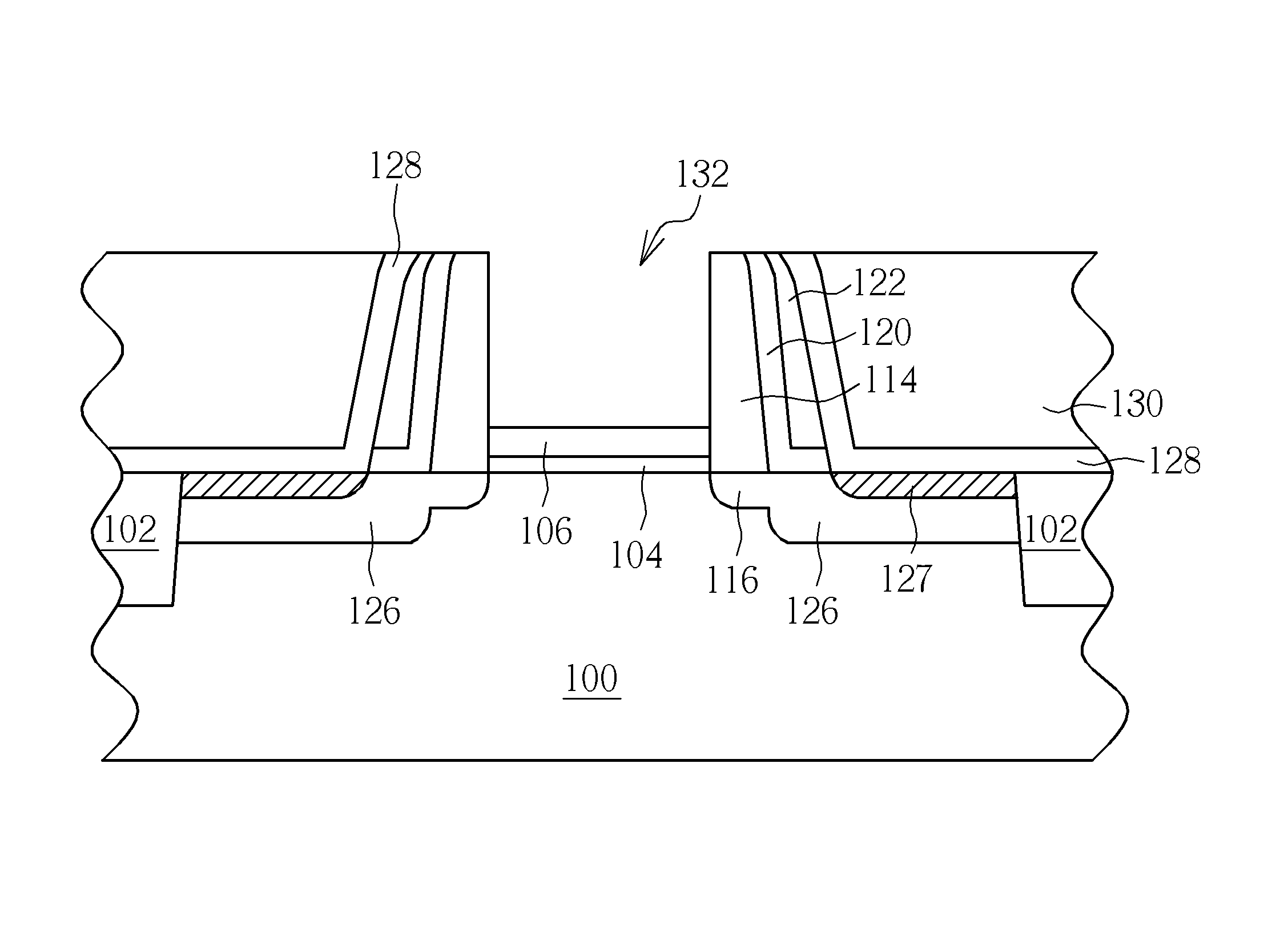
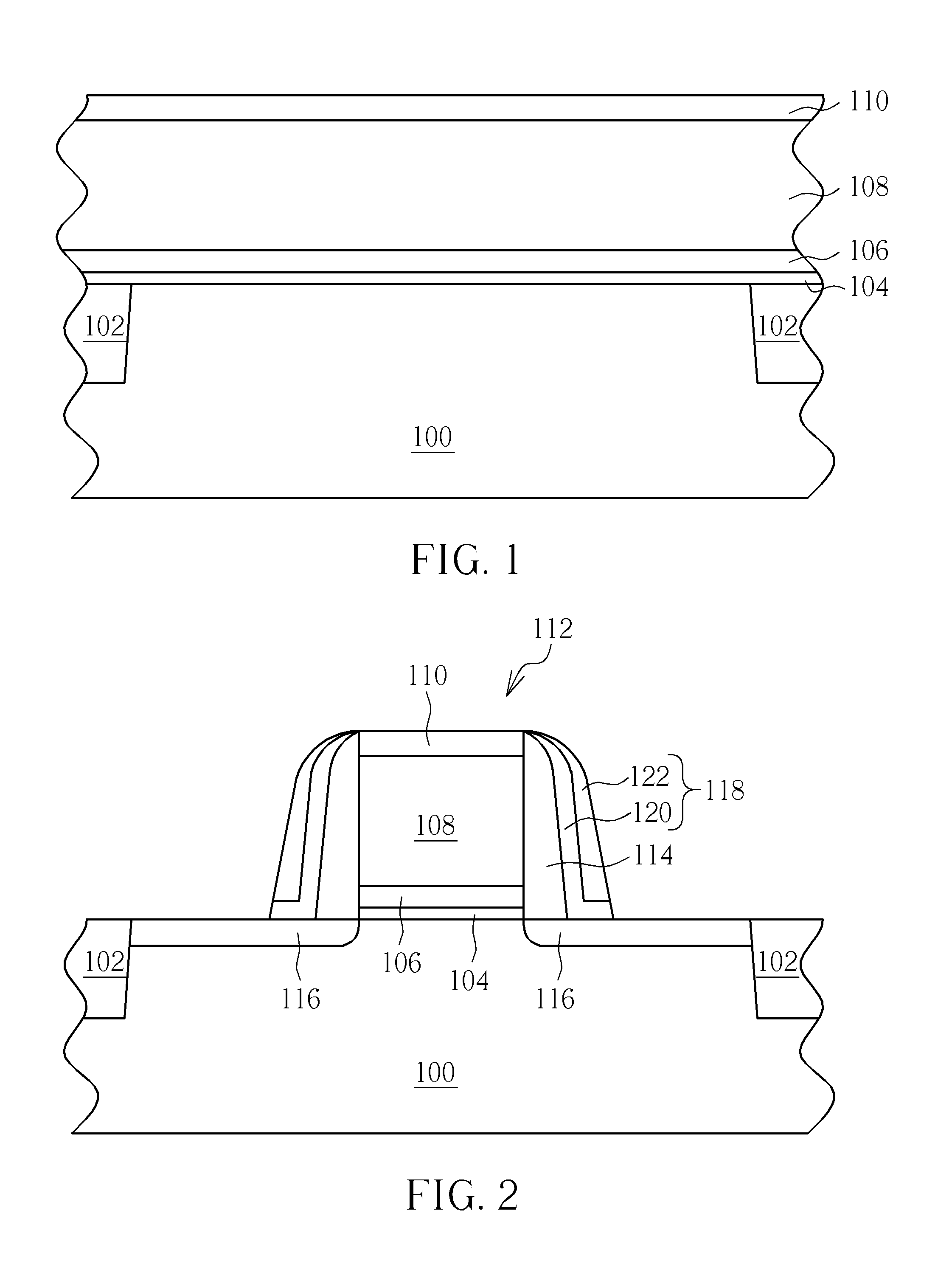
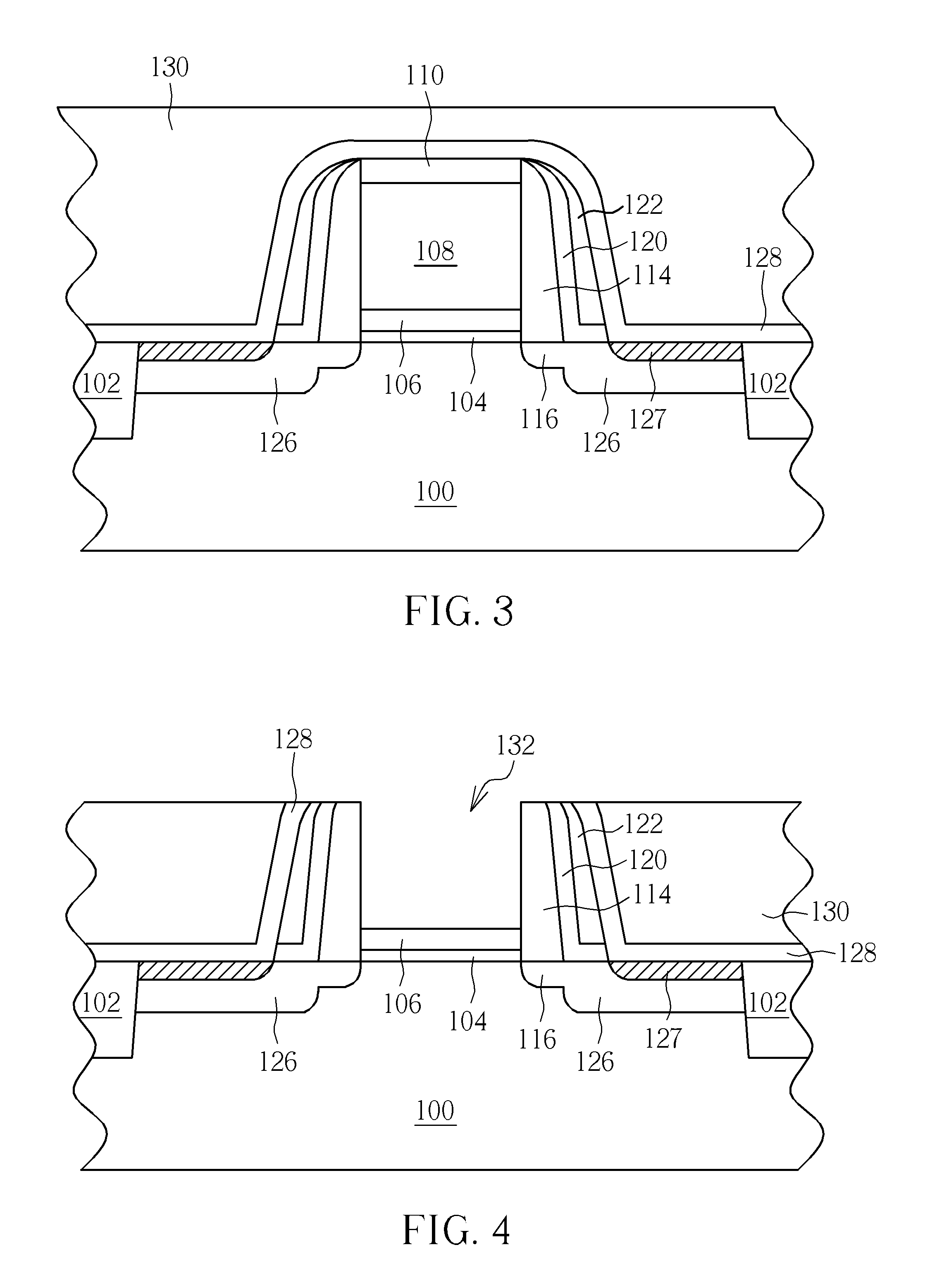
[0012]Referring to FIGS. 1-5, FIGS. 1-5 illustrate a method for fabricating a semiconductor device having metal gate. In this embodiment, the semiconductor device is preferably an NMOS transistor, in which the method preferably utilizes a gate-first approach accompanying a high-k first fabrication. As shown in FIG. 1, a substrate 100, such as a silicon substrate or a silicon-in-insulator (SOI) substrate is provided. A plurality of shallow trench isolations (STI) 102 used for electrical isolation is also formed in the substrate 100.
[0013]Next, an interfacial layer 104 composed of oxide or nitride is formed on the surface of the substrate 100. Next, a film stack composed of a high-k dielectric layer 106, a polysilicon layer 108, and a hard mask 110 is formed on the interfacial layer 104. Preferably, a barrier layer (not shown) could be formed on the high-k dielectric layer 106 and the polysilicon layer 108 is used as a sacrificial layer, which could be composed of undoped polysilicon,...
PUM
 Abstract
Description
Claims
Application Information
PatSnap Eureka turns technology decisions into work you can execute. Powered by our Innovation Knowledge Graph, it runs expert workflows across engineering, life sciences, materials and intellectual property. Get your review-ready output in minutes.


