Interlevel dielectric stack for interconnect structures

a dielectric stack and interconnect technology, applied in semiconductor devices, semiconductor/solid-state device details, thin material processing, etc., can solve the problems of difficult reduction of the thickness of the sicnh cap, inter-level dielectric stack flopping, etc., and achieve the effect of reducing the flow rate of the second vapor precursor

Active Publication Date: 2014-07-15
GLOBALFOUNDRIES US INC
View PDF8 Cites 6 Cited by
  • Summary
  • Abstract
  • Description
  • Claims
  • Application Information

AI Technical Summary

Benefits of technology

[0008]The present invention includes a dielectric stack and method of depositing the stack to a substrate using a single step deposition process. The dielectric stack includes a dense layer and a porous layer of the same elemental compound with different compositional atomic percentage, density, and porosity. The stack enhances mechanical modulus strength and enhances oxidation and copper diffusion barrier properties. The dielectric stack has inorganic or hybrid inorganic-organic random three-dimensional covalent bonding throughout the network, which contain different regions of different chemical compositions such as a cap component adjacent to a low-k component of the same type of material but with higher porosity.
[0011]According to a further aspect of the present invention, a method for forming a dielectric stack structure is provided. The method includes: introducing in a reactor a first vapor precursor of at least one of dimethylsilacyclopentane (DMSCP) and trimethylsilane (TMS) and a second vapor precursor of at least one of ammonia and nitrogen gas on a substrate; striking a plasma in the reactor; depositing a first layer of silicon, carbon, nitrogen and hydrogen on the substrate; reducing the flow rate of the second vapor precursor in the reactor; and depositing a second layer of silicon, carbon, nitrogen and hydrogen into the reactor.

Problems solved by technology

Furthermore, due to weak mechanical properties of the ultra-low k, flopping of the inter-level dielectric stack has been observed in high aspect ratio structures during fabrication.
Furthermore, the reduction of SiCNH cap thickness is difficult due to SiCOH and porous SiCOH dielectric is a poor Cu diffusion and oxidation barrier.

Method used


Image

  • Interlevel dielectric stack for interconnect structures
  • Interlevel dielectric stack for interconnect structures
  • Interlevel dielectric stack for interconnect structures

Examples


Embodiment Construction

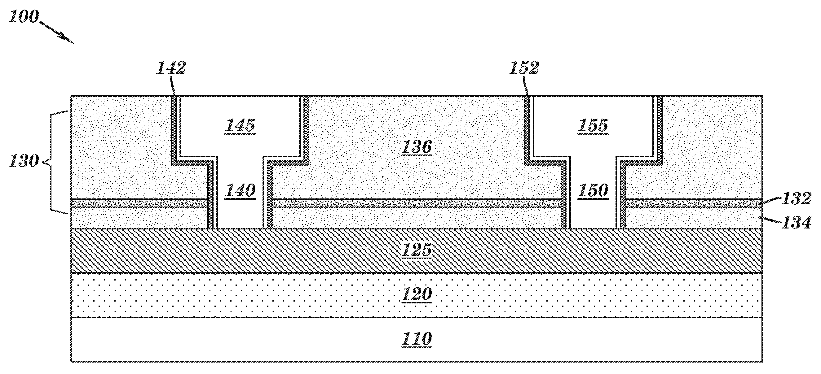
[0019]The following describes embodiments of the present invention with reference to the drawings. The embodiments are illustrations of the invention, which can be embodied in various forms. The present invention is not limited to the embodiments described below, rather representative for teaching one skilled in the art how to make and use it. Some aspects of the drawings repeat from one drawing to the next. The aspects retain their same numbering from their first appearance throughout each of the preceding drawings.

[0020]The present invention includes a dielectric stack and method of depositing the stack to a substrate using a single step deposition process. The dielectric stack includes a dense layer and a porous layer of the same elemental compound with different compositional atomic percentage, density, and porosity. The stack enhances mechanical modulus strength and enhances oxidation and copper diffusion barrier properties. The dielectric stack has inorganic or hybrid inorgani...


PUM

PropertyMeasurementUnit
dielectric constantaaaaaaaaaa
thicknessaaaaaaaaaa

Abstract

A dielectric stack and method of depositing the stack to a substrate using a single step deposition process. The dielectric stack includes a dense layer and a porous layer of the same elemental compound with different compositional atomic percentage, density, and porosity. The stack enhances mechanical modulus strength and enhances oxidation and copper diffusion barrier properties. The dielectric stack has inorganic or hybrid inorganic-organic random three-dimensional covalent bonding throughout the network, which contain different regions of different chemical compositions such as a cap component adjacent to a low-k component of the same type of material but with higher porosity.

Description

BACKGROUND OF THE INVENTION[0001]1. Field of the Invention[0002]The present invention relates to interconnect structures in semiconductor devices. More specifically, the present invention relates to an interlevel dielectric stack containing a dense layer and a porous layer of the same chemical composition.[0003]2. Description of the Related Art[0004]Current copper back end of the line interconnect fabrication requires the use of a copper cap, graded adhesion layer and intra / interlevel dielectric and SiCOH stack. As the stack and the interlevel dielectric thickness become smaller, the effective dielectric constant, k, of the stack becomes higher reducing the advantage of using an ultra-low k dielectric. Furthermore, due to weak mechanical properties of the ultra-low k, flopping of the inter-level dielectric stack has been observed in high aspect ratio structures during fabrication. In addition, the electrical breakdown of the porous SiCOH is worsening as the thickness is reduced belo...

Claims


Application Information

Patent Timeline
Patent Type & Authority Patents(United States)
IPC IPC(8): H01L29/40
CPCH01L21/76832H01L21/02274H01L21/76825H01L23/5329H01L23/5384H01L21/02167H01L21/76801H01L23/53295H01L21/76834H01L2924/0002Y10T428/249969H01L2924/00
Inventor NGUYEN, SON VANBONILLA, GRISELDAGRILL, ALFREDHAIGH, JR., THOMAS J.NITTA, SATYANARAYANA V.
Owner GLOBALFOUNDRIES US INC
Why Eureka
Try Eureka