

Semiconductor device and method for manufacturing the same
a semiconductor and semiconductor technology, applied in the direction of semiconductor devices, basic electric elements, electrical equipment, etc., can solve the problems of degrading electrical characteristics (typically, a short-channel effect) and becoming obvious, and achieve high integration, low power consumption, and high speed operation.
- Summary
- Abstract
- Description
- Claims
- Application Information
AI Technical Summary
Benefits of technology
Problems solved by technology
Method used
Image

Examples
embodiment 1
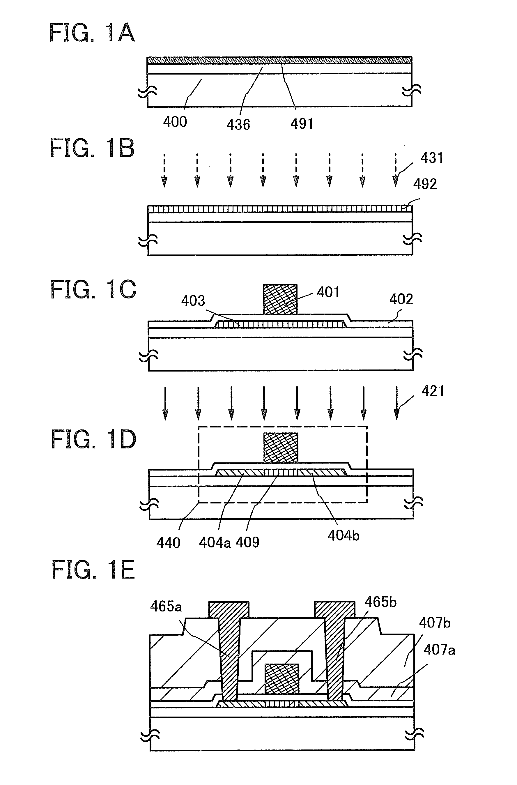
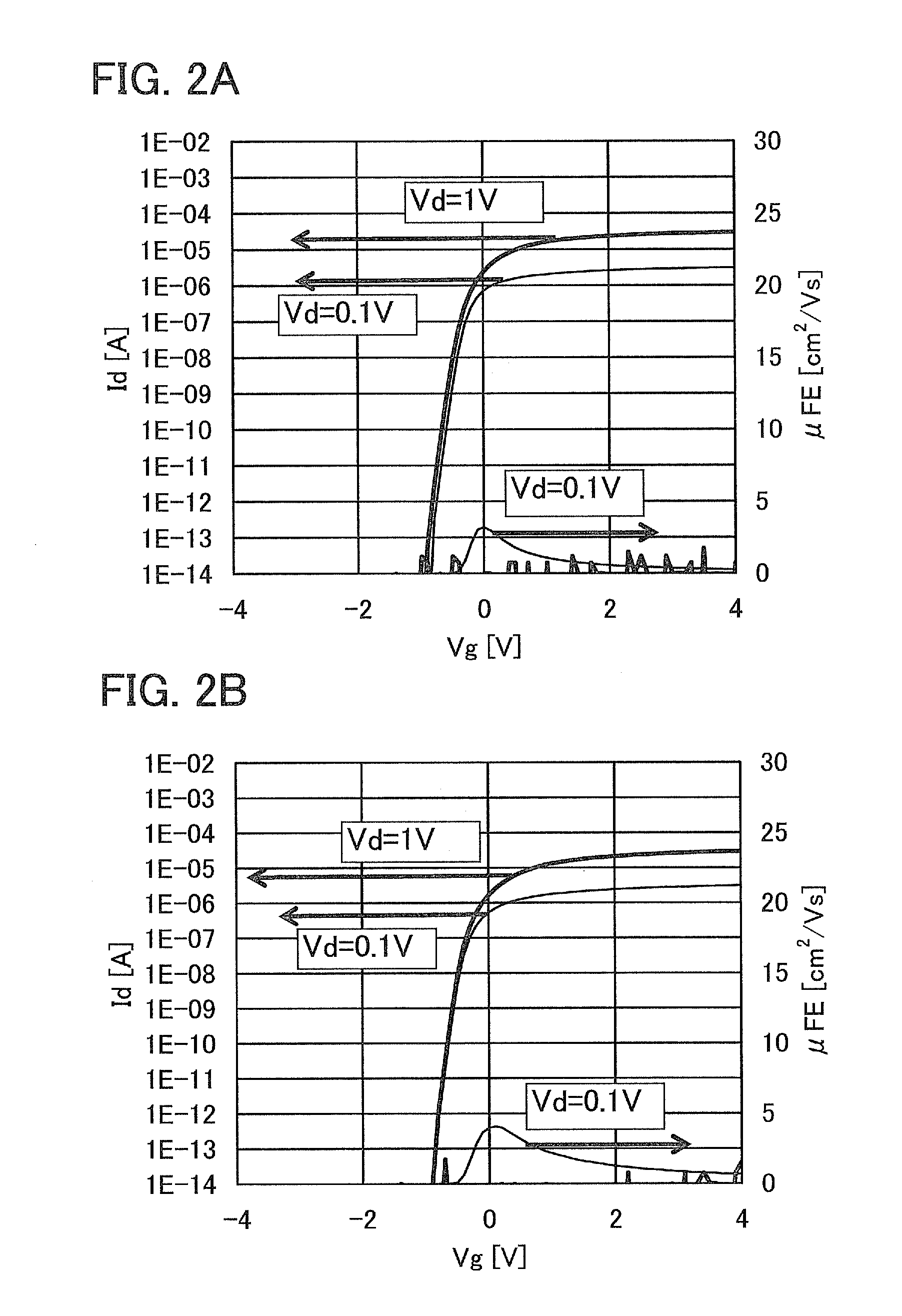
[0037]In this embodiment, one embodiment of a semiconductor device and a method for manufacturing the semiconductor device will be described with reference to FIGS. 1A to 1E. In this embodiment, a transistor including an oxide semiconductor film is described as an example of the semiconductor device.
[0038]The transistor may have a single-gate structure in which one channel formation region is formed, a double-gate structure in which two channel formation regions are formed, or a triple-gate structure in which three channel formation regions are formed. Alternatively, the transistor may have a dual-gate structure including two gate electrode layers positioned over and under a channel formation region with a gate insulating film provided therebetween.
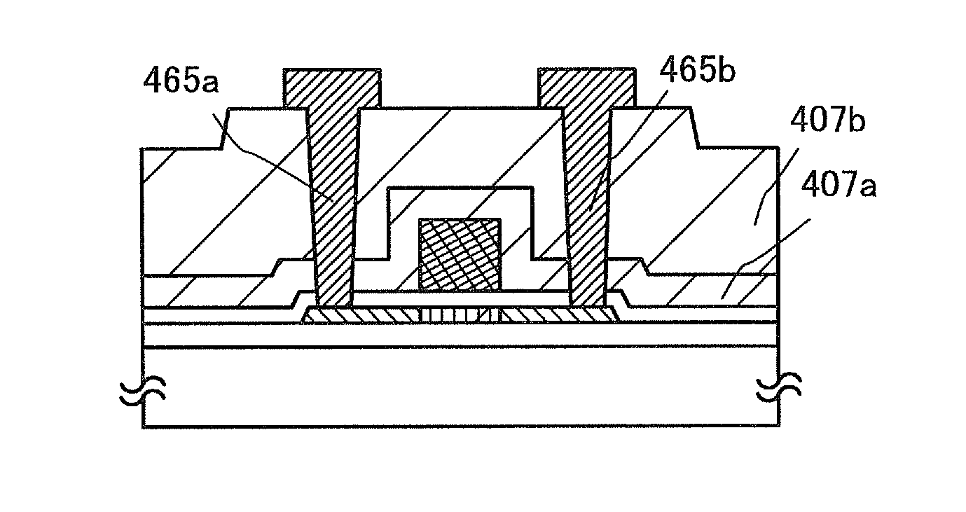
[0039]A transistor 440 illustrated in FIGS. 1A to 1E which also illustrate its manufacturing method is an example of a planar-type transistor having a top-gate structure.
[0040]The transistor 440 includes, over a substrate 400 having an in...
embodiment 2
[0156]In this embodiment, an example of a semiconductor device which includes the transistor described in this specification, which can hold stored data even when not powered, and which does not have a limitation on the number of write cycles, will be described with reference to drawings.
[0157]FIGS. 4A to 4C illustrate an example of the structure of a semiconductor device. FIGS. 4A to 4C illustrate a cross-sectional view, a plan view, and a circuit diagram, respectively, of the semiconductor device. Here, FIG. 4A corresponds to cross sections taken along line C1-C2 and line D1-D2 in FIG. 4B.
[0158]The semiconductor device illustrated in FIGS. 4A and 4B includes a transistor 160 including a first semiconductor material in a lower portion, and a transistor 162 including a second semiconductor material in an upper portion. The structure of the transistor described in Embodiment 1 can be applied to the transistor 162. The transistor 162 is an example in which an electrode layer 142a and ...
embodiment 3
[0189]In this embodiment, a semiconductor device which includes the transistor described in Embodiment 1 or 2, can hold stored data even when not powered, and does not have a limitation on the number of write cycles, and which has a structure different from the structure described in Embodiment 2 is described with reference to FIGS. 5A and 5B and FIGS. 6A to 6C.
[0190]FIG. 5A illustrates an example of a circuit configuration of a semiconductor device, and FIG. 5B is a conceptual diagram illustrating an example of a semiconductor device. First, the semiconductor device illustrated in FIG. 5A is described, and then, the semiconductor device illustrated in FIG. 5B is described.
[0191]In the semiconductor device illustrated in FIG. 5A, a bit line BL is electrically connected to a source electrode or a drain electrode of a transistor 162, a word line WL is electrically connected to a gate electrode of the transistor 162, and the source electrode or the drain electrode of the transistor 162...
PUM
 Abstract
Description
Claims
Application Information