Electrical contact for an energy-assisted magnetic recording laser sub-mount
- Summary
- Abstract
- Description
- Claims
- Application Information
AI Technical Summary
Benefits of technology
Problems solved by technology
Method used
Image

Examples
Embodiment Construction
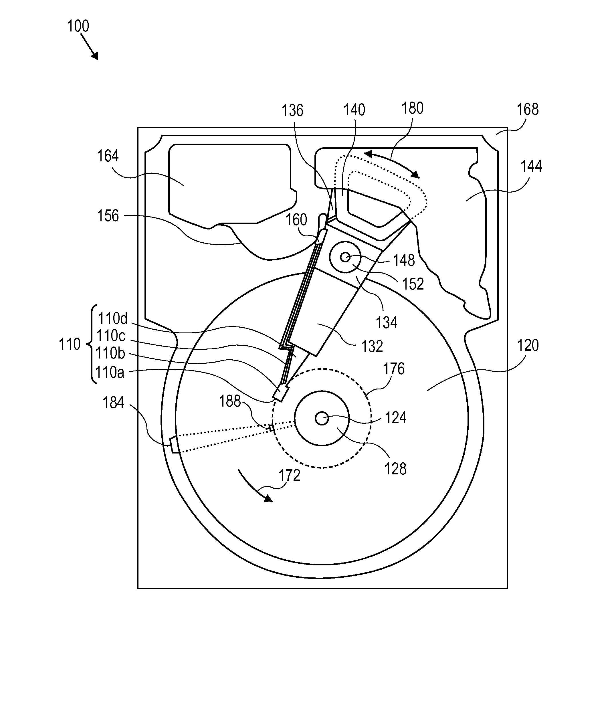
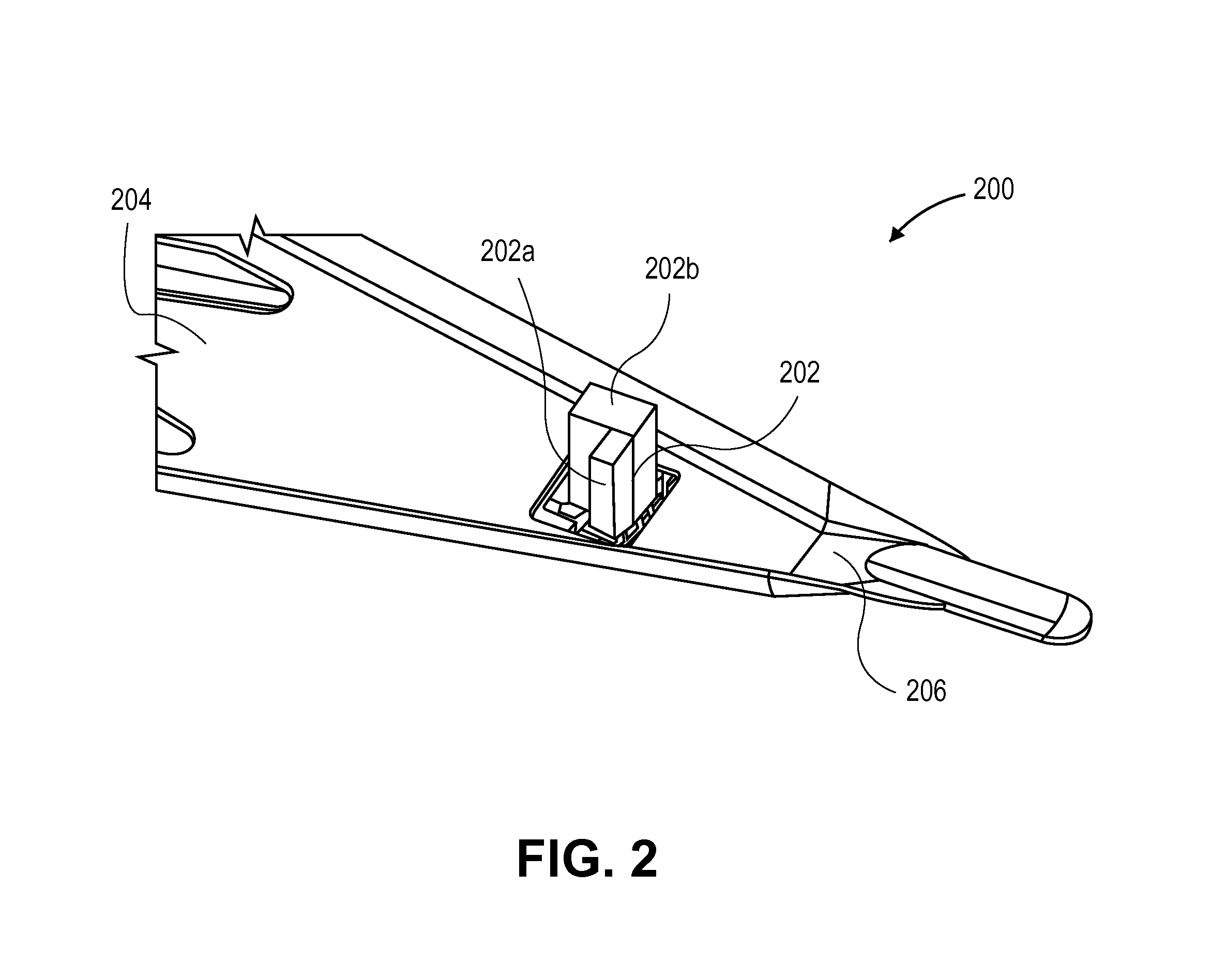
[0007]Embodiments of the invention are directed to electrically connecting a semiconductor laser module and a suspension that houses a head slider, in the context of a hard disk drive (HDD).
[0008]According to an embodiment, an energy-assisted magnetic recording (EAMR) assembly comprises a semiconductor laser module coupled with a suspension, where each of the suspension and a semiconductor laser sub-mount comprises respective electrical contacts used for fabricating an electrically conductive solder joint. Notably, the sub-mount electrical contact includes a metal barrier layer underneath an electrode layer, where the barrier layer material has a lower heat transfer coefficient than the sub-mount material. Consequently, during the soldering process the diffusion of heat to the sub-mount is inhibited and reduced, and the wettability of the solder is improved, thereby enabling a more robust and effective bond between the components.
[0009]Embodiments discussed in the Summary of Embodim...
PUM
 Abstract
Description
Claims
Application Information