Method for producing a microfabricated atomic vapor cell

a technology of atomic vapor cells and microfabricated materials, which is applied in the direction of liquid surface applicators, apparatus using atomic clocks, pretreated surfaces, etc., can solve the problems of affecting the stability of atomic clocks, hazardous methods, and complicated alkali metal vapor cell fabrication

Active Publication Date: 2014-12-09
CSEM CENT SUISSE DELECTRONIQUE & DE MICROTECHNIQUE SA RECH & DEV
View PDF2 Cites 65 Cited by
  • Summary
  • Abstract
  • Description
  • Claims
  • Application Information

AI Technical Summary

Benefits of technology

[0025]as a result, the method of alkali metal azide deposition is easily scalable to wafer-level filling.

Problems solved by technology

The difficulties encountered during the fabrication of vapor cells are related to the volatile character of alkali metals and to the reactivity of alkali metals with oxygen.
As a result, all handling of alkali metals has to be done either under high vacuum conditions or in an anaerobic atmosphere, a fact that complicates the fabrication of alkali metal vapor cells.
A disadvantage of such method is that unreacted Ba tends to form different forms of nitride with the released nitrogen, causing pressure fluctuation inside the cell which affects the stability of the atomic clock, as disclosed by S. Knappe et al. in the publication “Atomic vapor cells for chipscale atomic clocks with improved long-term frequency stability”, Opt. Lett. 30, 2351-3.
However, this method is hazardous since, for thermal evaporation, the azide has to be heated above its melting point, favoring uncontrolled decomposition and explosion.
For batch fabrication, the cell filling by manually placing solid crystals of alkali metal azide into cavities is cumbersome and an accurate control of the deposited amount of azide is impossible.
The method described in the publication of Li-Anne Liew et al. cited above solves some of these challenges but suffers from cost and danger related disadvantages.

Method used


Image

  • Method for producing a microfabricated atomic vapor cell

Examples


example

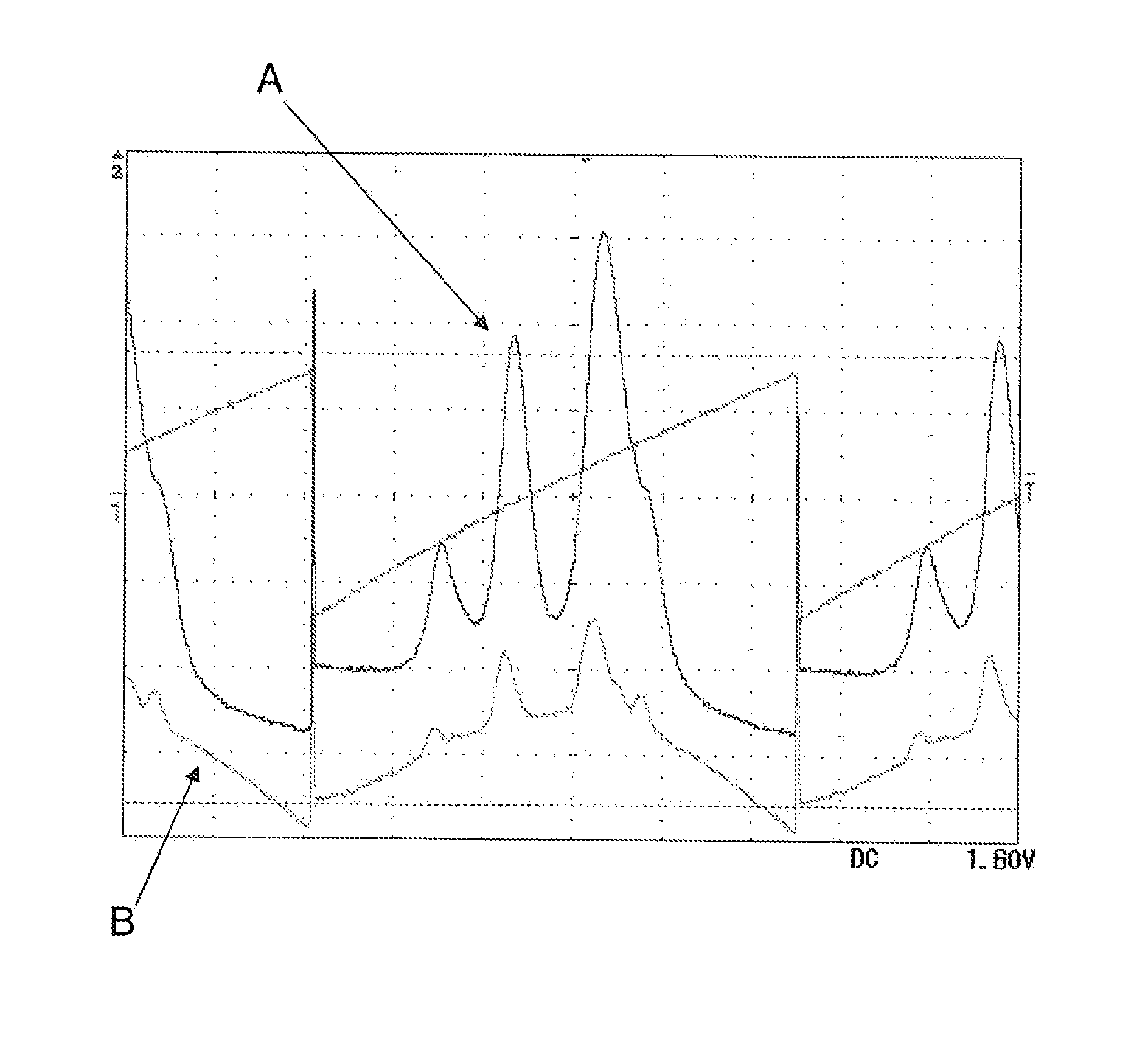
[0069]A quantity of 100 mg of RbN3 was deposited in a polypropylene vial, and 1 ml of DI water was filled into the vial. The vial was then agitated until the RbN3 was completely dissolved after about 1 min. A Gilson micropipette, model P2, was adjusted to a quantity of 200 nl. Using the micropipette and a polypropylene barrier tip mounted onto it, 200 nl of aqueous solution was taken from the vial and deposited into a cavity formed by pits etched into a silicon wafer and closed at the bottom by a glass wafer. The dimensions of the cavities were 5×5×1 mm3. The step of pipetting was repeated until dissolved rubidium azide solution was dispensed in all cavities of the wafer. The stack of the bonded wafer pair was then placed on the chuck of the bonding machine, and a top glass wafer was positioned above the stack on 3 flags which are used to separate the top glass wafer from the stack of the already bonded wafer pair. The bonding chuck was then placed in the bonding machine. The chambe...


PUM


Abstract

The present invention relates to a method for producing a microfabricated atomic vapor cell, including a step of forming at least one cavity in a substrate and closing the cavity at one side. The method further includes: —a step of depositing a solution including an alkali metal azide dissolved in at least one of its solvents, —a step of evaporating such solvent for forming a recrystallized alkali metal azide, —a step of decomposing the recrystallized alkali metal azide in an alkali metal and nitrogen, such alkali metal depositing in the cavity of the substrate.

Description

TECHNICAL FIELD[0001]The present invention relates to a method for producing a microfabricated atomic vapor cell, comprising a step of forming at least one cavity in a substrate.BACKGROUND OF THE INVENTION[0002]Miniaturized atomic clocks characterized by a small size and a drastically reduced power consumption compared to standard atomic clocks exhibit an increasing interest mainly for applications in portable devices. The unprecedented frequency stability of atomic clocks is achieved by a suitable interrogation of optically excited atoms which takes place in the so-called vapor cell, the heart of an atomic clock. The vapor cell consists of a sealed cavity which contains small amounts of an alkali metal, preferably rubidium or cesium, a buffer gas and / or an anti-relaxation coating. MEMS (Microelectromechanical systems) technology allows the fabrication of miniaturized vapor cells having a volume in the range of a few cubic millimeters. The fabrication of vapor cells typically consis...

Claims


Application Information

Patent Timeline
Patent Type & Authority Patents(United States)
IPC IPC(8): G04F5/14B05D3/02B05D7/22B05D3/06B05D3/04
CPCG04F5/14
Inventor OVERSTOLZ, THOMASHAESLER, JACQUESSPASSOV, VLADISLAV
Owner CSEM CENT SUISSE DELECTRONIQUE & DE MICROTECHNIQUE SA RECH & DEV
Why Eureka
Try Eureka