Member for semiconductor manufacturing apparatus

a manufacturing apparatus and semiconductor technology, applied in the direction of electric devices, basic electric elements, electrostatic holding devices, etc., can solve the problems of high residual stress at the time of joining and insufficient joint strength

Active Publication Date: 2014-12-09
NGK INSULATORS LTD
View PDF10 Cites 1 Cited by
  • Summary
  • Abstract
  • Description
  • Claims
  • Application Information

AI Technical Summary

Benefits of technology

[0008]The present invention has been made to solve such problems. Accordingly, the main object of the present invention is to provide a member for a semiconductor manufacturing apparatus, wherein the residual stress at the time of joining is reduced, cracking does not occur in a ceramic substrate, and sufficient joint strength is obtained even when an operation temperature is 200° C.
[0018]According to this member for a semiconductor manufacturing apparatus, the residual stress at the time of joining is reduced, cracking does not occur in a ceramic substrate having a reduced thickness, and sufficient joint strength is obtained even when an operation temperature is 200° C. That is, the member for a semiconductor manufacturing apparatus according to the present invention can be used at room temperature to 200° C. and, therefore, can respond to needs for higher temperatures required of electrostatic chuck and the like in recent years.
[0020]Regarding the member for a semiconductor manufacturing apparatus according to the present invention, it is preferable that the above-described joining layer contains an intermetallic compound phase generated through reaction between a metal contained in a metallized layer covering a predetermined region including the above-described exposed electrode portion before joining and elements other than Au in the above-described joining material. In addition, it is preferable that a Au-rich phase generated by consumption of the elements other than Au in the above-described joining material through reaction with the metal contained in the above-described metallized layer is contained. This Au-rich phase has advantages that the electrical resistance is low, so as to reduce an electric power loss at the time of feeding of an electric power, the residual stress at the time of joining is relaxed easily because of being soft, and the heat resistance can be enhanced because the melting point is raised as the Au concentration increases through reaction at the time of joining.
[0023]Regarding the member for a semiconductor manufacturing apparatus according to the present invention, when the value of a clearance, which is the value calculated by subtracting the diameter of the power feed member from the diameter of a hole in the ceramic substrate, is represented by C, it is preferable that the C / R ratio of C to the diameter R of the hole of the above-described ceramic substrate satisfies C / R≦0.15. In this case, when C / R≦0.15 is satisfied, the joint strength between the ceramic substrate and the power feed member becomes high as compared with that in the case where C / R is out of this range. In addition, the ceramic substrate and the power feed member are preferably selected in such a way that the thermal expansion coefficient difference D satisfies −2.2≦D≦0 (unit: ppm / K), and are more preferably selected in such a way that the −2.2≦D≦−1.0 (unit: ppm / K) is satisfied. Consequently, the joint strength is more enhanced because a state in which the power feed member is shrinkage-fitted to the ceramic substrate with the joining layer therebetween can be brought about. Meanwhile, in the case where C / R 0.15 is satisfied, if the value of C / R is large, it is difficult to arrange the power feed member at the center of the hole in the ceramic substrate well. As a result, strength variations occur easily. Therefore, it is preferable that C / R≦0.09 is satisfied in order to obtain a joining body having higher strength, less variations, and high reliability.
[0029]According to the method for manufacturing the member for a semiconductor manufacturing apparatus according to the present invention, the above-described member for a semiconductor manufacturing apparatus according to the present invention can be produced easily. In this regard, the temperature in the heating in the step (c) may be set appropriately at a temperature, at which peeling does not occur at the joining interface and cracking does not occur in the ceramic substrate, in accordance with the thermal expansion coefficient difference D. However, 200° C. to 500° C. is desirable, and in particular 250° C. to 420° C. is preferable because the residual stress in the vicinity of the joining interface increases as the heating temperature becomes high.

Problems solved by technology

Under such circumstances, there is a problem in that the melting point of indium is low and, therefore, in the case where the operation temperature is 150° C. to 200° C., sufficient joint strength is not obtained.
Therefore, there is a problem in that a residual stress at the time of joining becomes high.

Method used


Image

  • Member for semiconductor manufacturing apparatus
  • Member for semiconductor manufacturing apparatus
  • Member for semiconductor manufacturing apparatus

Examples


examples

[1] Production of Specimen

[1-1] Production Procedure of Specimen S1

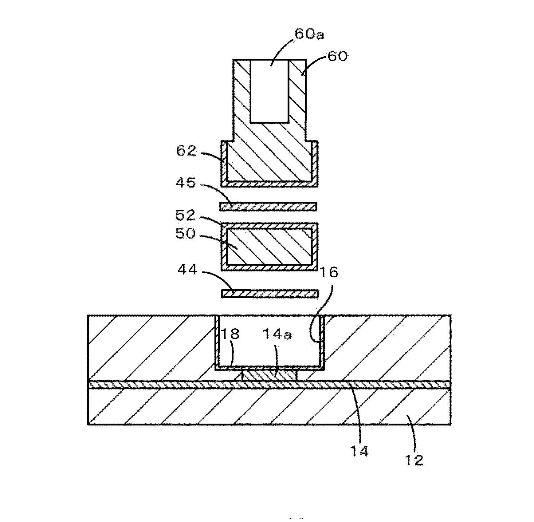
[0060]Specimen S1 simulating the joining structure shown in FIG. 2 was produced as described below. FIG. 6 is a perspective exploded view of Specimen S1. Initially, a concave portion 74 having a diameter of 6.00 mm and a depth of 0.5 mm was formed in a ceramic substrate 72 having a length of 20 mm, a width of 20 mm, and a thickness of 5 mm. Thereafter, the inside of the concave portion was subjected to a roughing treatment through sandblast, and about 3 μm of electroless Ni plating was applied. As for the material for the ceramic substrate 72, alumina (Al2O3), aluminum nitride (AlN), yttria (Y2O3), silicon carbide (SiC), and magnesia (MgO) were used. Furthermore, a power feed member 76 having a diameter of 5.95 mm and a height of 6 mm and a joining material 78 having a diameter of 5.8 mm and a foil thickness of 100 μm were prepared. Moreover, the value of the C / R ratio of a clearance C calculated by subtracting the d...


PUM

PropertyMeasurementUnit
temperatureaaaaaaaaaa
melting pointaaaaaaaaaa
temperaturesaaaaaaaaaa

Abstract

An electrostatic chuck is provided with a ceramic substrate 12 in which an electrode 14 is embedded, an electrode terminal 14a exposed at the bottom of a concave portion 16 disposed on the back surface of the ceramic substrate 12, a power feed member 20 to supply an electric power to the electrode 14, and a joining layer 22 to connect this power feed member 20 to the ceramic substrate 12. The joining layer 22 is formed by using a AuGe based alloy, a AuSn based alloy, or a AuSi based alloy. The ceramic substrate 12 and the power feed member 20 are selected in such a way that the thermal expansion coefficient difference D calculated by subtracting the thermal expansion coefficient of the ceramic substrate 12 from the thermal expansion coefficient of the power feed member 20 satisfies −2.2≦D≦6 (unit: ppm / K).

Description

BACKGROUND OF THE INVENTION[0001]1. Field of the Invention[0002]The present invention relates to a member for a semiconductor manufacturing apparatus.[0003]2. Description of the Related Art[0004]In the field of semiconductor manufacturing apparatuses, alumina (Al2O3), aluminum nitride (AlN), and the like, which are dense ceramic, are used as a substrate for an electrostatic chuck. Production is performed in such a way that a high-frequency electrode is embedded in a ceramic substrate in order to generate plasma for semiconductor processing. Here, it is necessary that the electrode embedded in the ceramic substrate is electrically joined to a power feed terminal. As for this power feed terminal, a metal material having excellent electrical conductivity is used favorably. In general, the metal material has a large thermal expansion coefficient as compared with that of the ceramic. Therefore, in order to produce a product by being joined to the ceramic substrate, it is required that cr...

Claims


Application Information

Patent Timeline
Patent Type & Authority Patents(United States)
IPC IPC(8): H01L21/683H02N13/00
CPCH01L21/6833H01L21/687
Inventor KIDA, MASAHIROHAYASE, TORUKATSUDA, YUJI
Owner NGK INSULATORS LTD
Why Eureka
Try Eureka