

Semiconductor device
a technology of semiconductors and devices, applied in the direction of semiconductor devices, electrical equipment, transistors, etc., can solve the problems of manufacturing power devices, and achieve the effect of suppressing the reduction of on-state current and high breakdown voltage characteristics
- Summary
- Abstract
- Description
- Claims
- Application Information
AI Technical Summary
Benefits of technology
Problems solved by technology
Method used
Image

Examples
embodiment 1
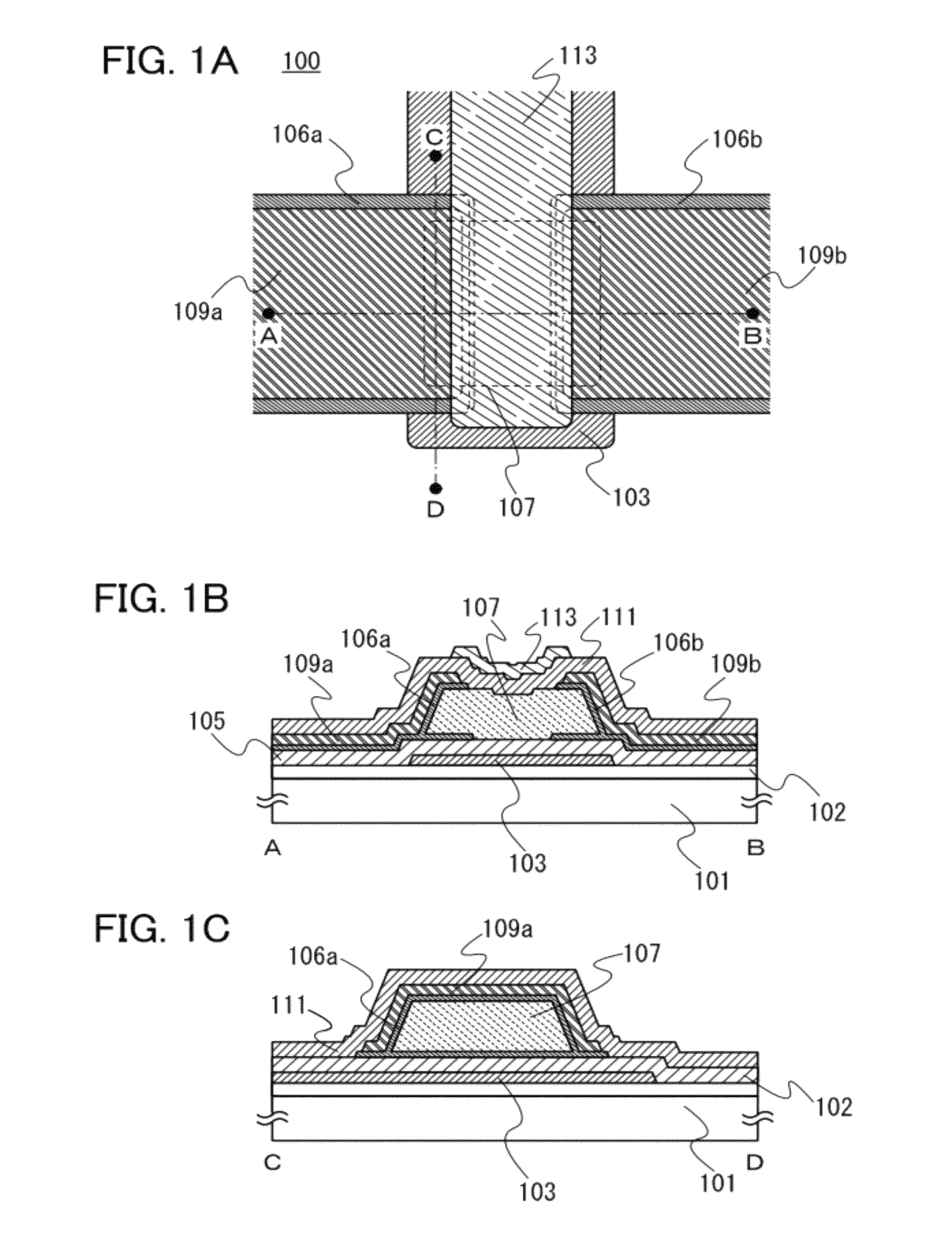
[0053]In this embodiment, a structure of a transistor and a method for manufacturing the transistor according to one embodiment of the present invention will be described with reference to FIGS. 1A to 1C, FIGS. 2A to 2D, and FIGS. 3A to 3D.
100>
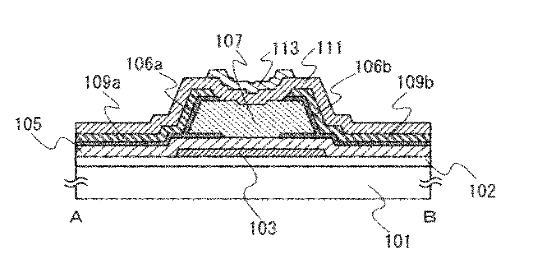
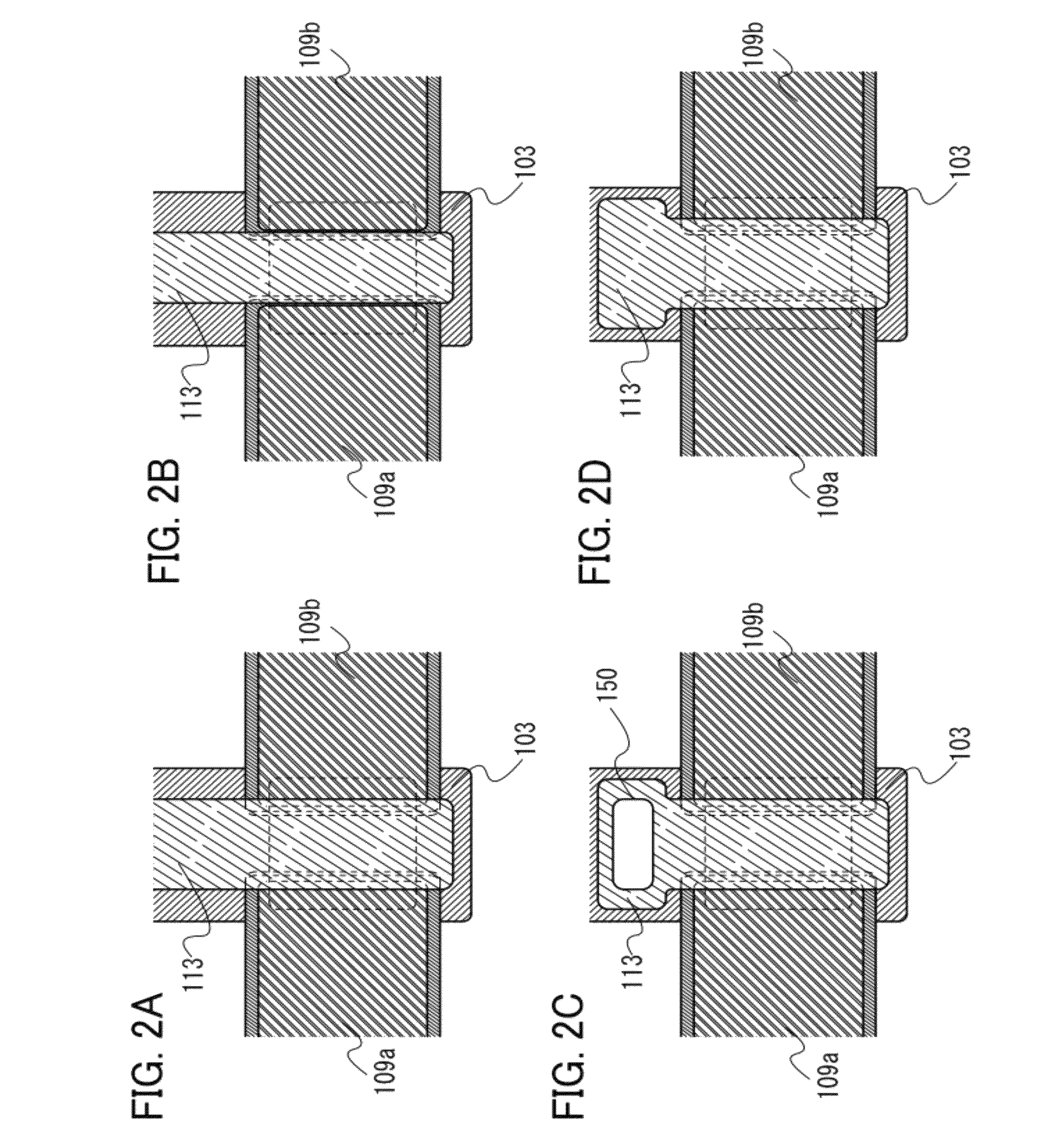
[0054]FIG. 1A is a plan view of a transistor 100. Note that a base insulating layer 102, a gate insulating layer 105, and an insulating layer 111 are not illustrated in FIG. 1A for convenience. FIG. 1A illustrates a first gate electrode 103 functioning as a gate electrode, an oxide semiconductor layer 107 functioning as a channel formation region, oxide semiconductor layers 106a and 106b having high carrier density, a source electrode 109a, a drain electrode 109b, and a second gate electrode 113 which is provided between the source electrode 109a and the drain electrode 109b, which overlaps with the oxide semiconductor layer 107 with the insulating layer 111 interposed therebetween, and which functions as a back gate electrode. In other words,...
embodiment 2
[0140]In this embodiment, a transistor 200 having a structure which is partly different from the structure of the transistor 100 described in Embodiment 1 will be described.
[0141]In the transistor 200 described in this embodiment, the oxide semiconductor layer 107 of the transistor 100 described in Embodiment 1 includes a crystalline oxide semiconductor. The crystalline oxide semiconductor can be formed by the following two types of methods.
[0142]One method is to form a crystalline oxide semiconductor film in such a way that an oxide semiconductor is formed twice and heat treatment is performed twice (this method is referred to as a method 1 for convenience), whereas the other is to form a crystalline oxide semiconductor film in such a way that a substrate is heated when an oxide semiconductor is formed (this method is referred to as a method 2 for convenience). Note that the crystalline oxide semiconductor film obtained by any of the above methods has a region in which crystals are...
embodiment 3
[0158]In this embodiment, an application of the transistor described in any of the embodiments will be described. The transistor described in any of the embodiments can be used as a power device to protection circuits of batteries of various electronic devices, for example.
[0159]An example of an application in which the transistor described in any of the embodiments is used as part of a protection circuit is described with reference to FIGS. 9A and 9B.
[0160]FIG. 9A illustrates an electromagnetic cooker 1000. The electromagnetic cooker 1000 heats cookware and the like by using electromagnetic induction generated by current flowing through a coil unit 1001. The electromagnetic cooker 1000 includes a battery 1002 for supplying current that is to flow through the coil unit 1001, a semiconductor device 1003 in which the transistor of one embodiment of the present invention serves as part of a protective circuit, and a solar battery 1004 for charging the battery 1002. Note that FIG. 9A il...
PUM
 Abstract
Description
Claims
Application Information