Atomic layer deposition lithography

a lithography and layer technology, applied in the field of atomic layer deposition lithography process, can solve the problems of inability to successfully transfer structures onto the substrate surface, the lithography process has become more and more difficult to achieve precisely and accurately transfer even small features onto the substrate, and the integration circuit has evolved into complex devices

Inactive Publication Date: 2015-01-13
APPLIED MATERIALS INC
View PDF9 Cites 201 Cited by
  • Summary
  • Abstract
  • Description
  • Claims
  • Application Information

AI Technical Summary

Problems solved by technology

Integrated circuits have evolved into complex devices that can include millions of components (e.g., transistors, capacitors and resistors) on a single chip.
Accordingly, the lithography process has become more and more challenging to transfer even smaller features onto a substrate precisely and accurately without damage.
However, at such small dimensions, the collapse or damage of the photoresist layer often occurs during the subsequent etching process, resulting in failure to successfully transfer structures onto a substrate surface.
As the feature sizes formed on microelectronic device continue to shrink, the aqueous base solution developer may become problematic due to image collapse caused by the capillary forces and surface tension of water.
Furthermore, solution based developers tend to leave undesired contaminates on the substrate after the development process, thereby adversely effecting the substrate cleanliness.

Method used


Image

  • Atomic layer deposition lithography
  • Atomic layer deposition lithography
  • Atomic layer deposition lithography

Examples


Embodiment Construction

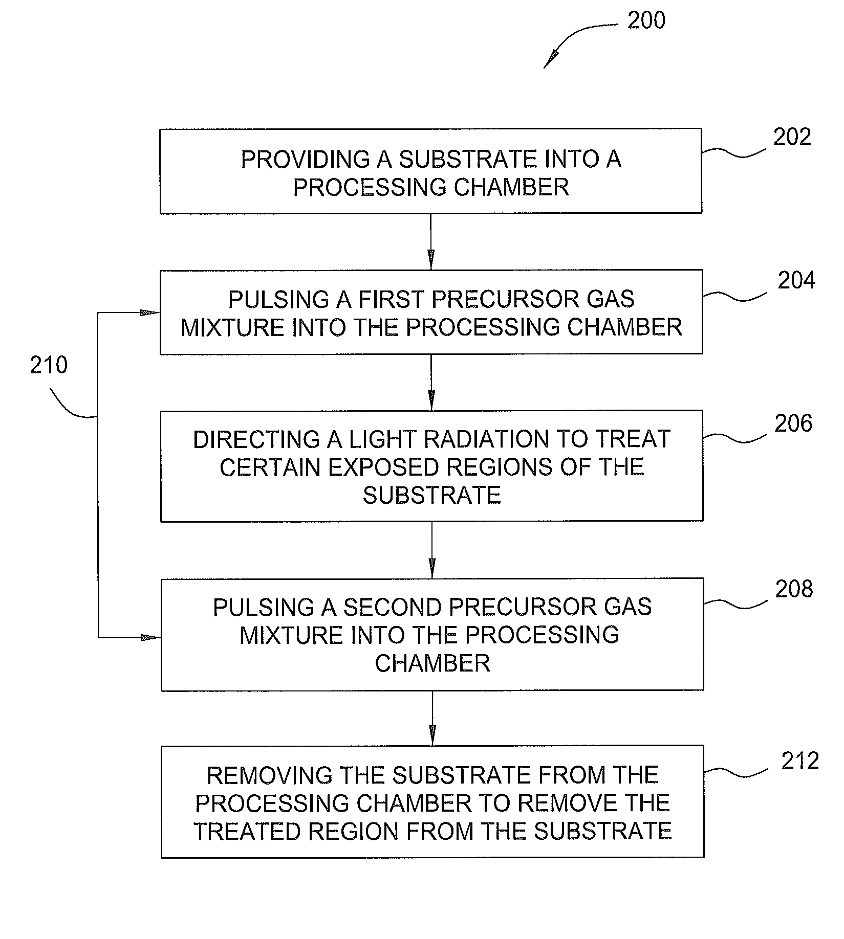
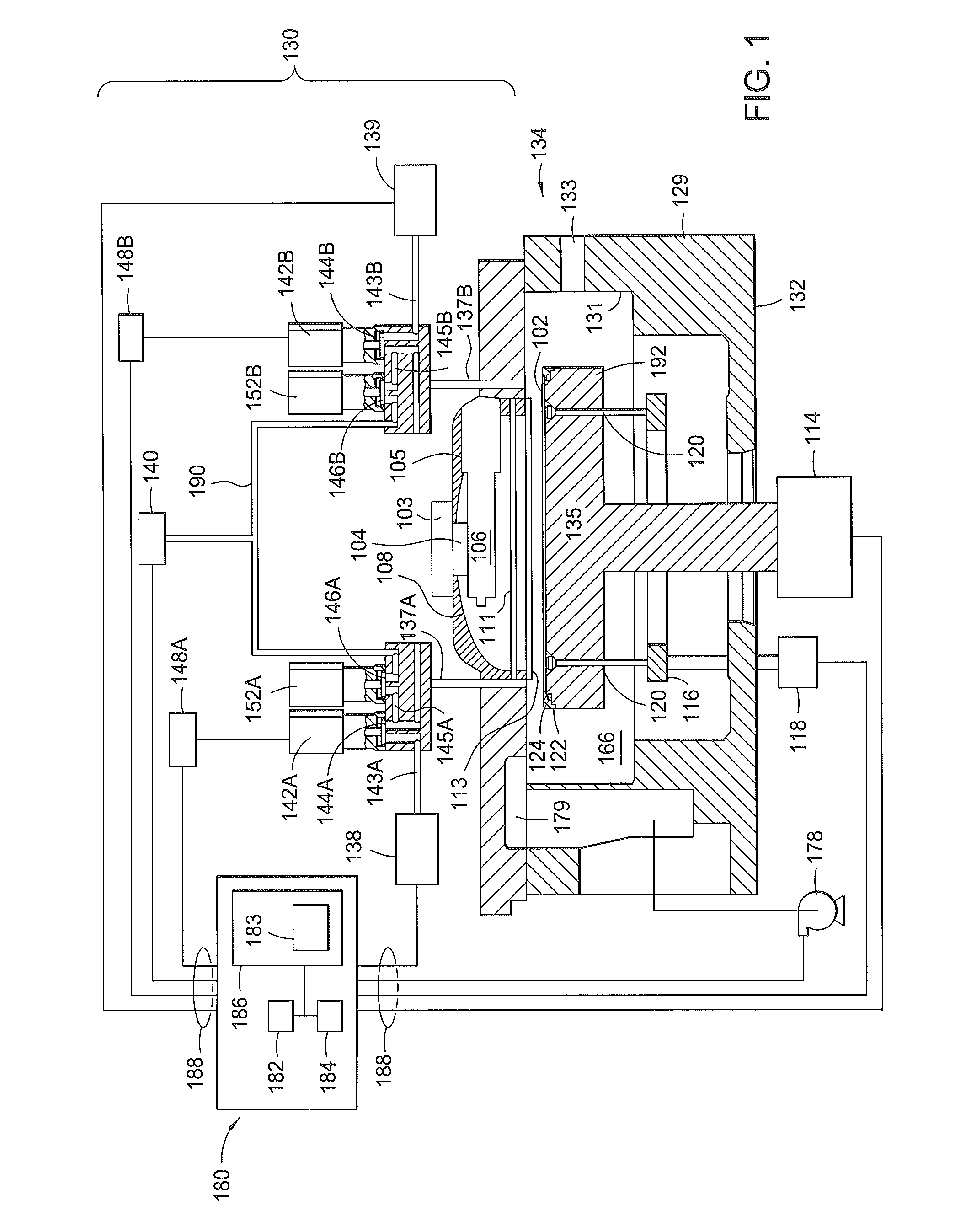
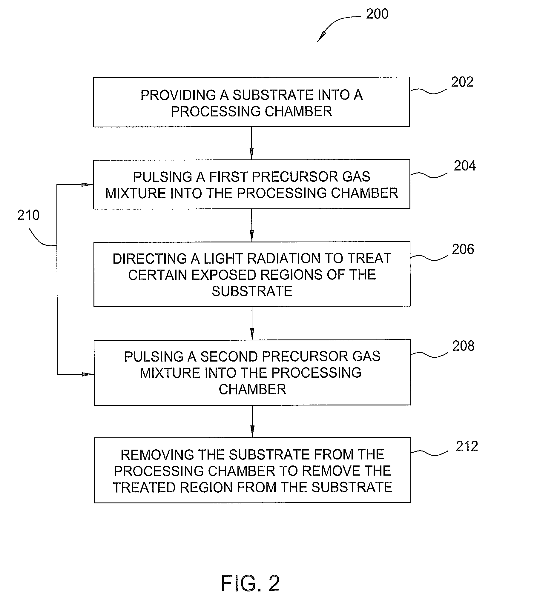
[0018]Methods and an apparatus for performing an atomic layer deposition (ALD) lithography process are provided in the present disclosure. The ALD lithography process utilizes an ALD process along with a lithography process to form features onto a substrate surface without using a conventional photoresist layer and / or a hardmask layer. The ALD lithography processing chamber provides a dual function; to deposit an atomic layer deposited layer and to perform a lithography process (e.g., energy beam treatment process) to form features / structures on the atomic layer deposited layer. The substrate may include one or more nonconductive materials, such as silicon, silicon oxide, doped silicon, germanium, gallium arsenide, glass, and sapphire. The substrate may also include dielectric materials such as silicon dioxide, organosilicates, and carbon doped silicon oxides. Further, the substrate can include any other materials such as metal nitrides and metal alloys, depending on the application...


PUM

PropertyMeasurementUnit
wavelengthaaaaaaaaaa
diametersaaaaaaaaaa

Abstract

Methods and apparatus for performing an atomic layer deposition lithography process are provided in the present disclosure. In one embodiment, a method for forming features on a material layer in a device includes pulsing a first reactant gas mixture to a surface of a substrate disposed in a processing chamber to form a first monolayer of a material layer on the substrate surface, directing an energetic radiation to treat a first region of the first monolayer, and pulsing a second reactant gas mixture to the substrate surface to selectively form a second monolayer on a second region of the first monolayer.

Description

RELATED APPLICATIONS[0001]This application claims priority to U.S. Patent Application Ser. No. 61 / 601,511, filed on Feb. 21, 2012, which is incorporated by reference in its entirety.BACKGROUND[0002]1. Field[0003]The present invention generally relates to methods and an apparatus for an atomic layer deposition lithography process, more specifically, to methods and an apparatus for utilizing an atomic layer deposition process along with a lithography process to form features / structures on a substrate surface in the semiconductor field.[0004]2. Description of the Related Art[0005]Integrated circuits have evolved into complex devices that can include millions of components (e.g., transistors, capacitors and resistors) on a single chip. The evolution of chip designs continually requires faster circuitry and greater circuit density. The demands for greater circuit density necessitate a reduction in the dimensions of the integrated circuit components.[0006]As the dimensions of the integrat...

Claims


Application Information

Patent Timeline
Patent Type & Authority Patents(United States)
IPC IPC(8): G03F7/26G03F7/16
CPCG03F7/16G03F7/0035G03F7/165G03F7/167H01L21/0274
Inventor WU, BANQIUKUMAR, AJAYNALAMASU, OMKARAM
Owner APPLIED MATERIALS INC
Why Eureka
Try Eureka