Optical waveguide board having guided structure and method of manufacturing the same, and method of manufacturing optical-electrical hybrid board

a technology of optical waveguides and waveguides, which is applied in the direction of instruments, other domestic objects, optical elements, etc., can solve the problems of increasing the number of wirings and countermeasures for crosstalk with conventional electrical wirings, and achieves the effects of increasing optical loss, simple technique, and high yield ratio

Inactive Publication Date: 2015-01-27
RESONAC CORPORATION
View PDF24 Cites 3 Cited by
  • Summary
  • Abstract
  • Description
  • Claims
  • Application Information

AI Technical Summary

Benefits of technology

[0017]By using a manufacturing method according to the present invention, a metal film can be formed on a tapered part of a mirror pattern and guiding patterns in a state that a mask member having a through hole at a desired position and the guiding patterns provided simultaneously with formation of the mirror pattern are guided by mating. Thereby, because a conventional photo-lithography step using a resist film and the like is unnecessary, a mirror part of an optical waveguide can be fabricated with a simple technique with a high yield ratio. Also, by separating a step of fabricating the mirror part and an optical reflective film, and a step of forming a wiring core, there is not a risk that an optical reflective film may adhere to an end surface of an optical waveguide when forming the reflective film; therefore, it becomes possible to form a slope surface of a mirror and an end surface of an optical waveguide in proximity, and a possibility of concern about an increase of optical loss due to beam divergence of light incident on and emitted from an end surface of an optical waveguide can be avoided. Also, by forming the wiring core by lithography with reference to the guiding patterns provided simultaneously with formation of the mirror pattern, it becomes easy to form a mirror pattern and the wiring core relatively with high guiding accuracy of μm order. Furthermore, by forming a clad layer, the mirror pattern, and the wiring core by repeating lamination and working to build them up sequentially on a board using the manufacturing method, an optical wiring can be fabricated with processes on a consistent board; therefore, significant reduction in the numbers of parts and steps can be achieved, and it is advantageous in multilayer formation.
[0018]Furthermore, by a manufacturing method of, simultaneously with formation of a second guiding pattern on the clad layer on the guiding patterns, respectively forming a third guiding pattern on the clad layer on the mirror pattern, and then placing optical devices having concave shapes or an optical module board on which the optical devices are respectively mounted, an optical-electrical hybrid board in which the optical devices, the mirror pattern, and the wiring core can be optically connected simply with high guiding accuracy of μm order due to the third guiding pattern is completed.
[0019]As a result, the present invention provides an effect that it is possible to provide a guided structure provided in an optical waveguide and an optical connection part in an optical waveguide board that transmits high-speed optical signals transmitted and received between chips and between boards in equipment such as a rack, and an optical-electrical hybrid board that performs bulk processing of the transmitted and received optical signals on the board, that can reduce parts, simplify steps, and be fabricated with high guiding accuracy and a high yield ratio, and a method of manufacturing a board using the same.

Problems solved by technology

When systems handle further larger capacities from now on, and a device processes information of Tbps or more, problems such as the number of wirings and countermeasures for crosstalk become more serious with conventional electrical wirings.

Method used


Image

  • Optical waveguide board having guided structure and method of manufacturing the same, and method of manufacturing optical-electrical hybrid board
  • Optical waveguide board having guided structure and method of manufacturing the same, and method of manufacturing optical-electrical hybrid board
  • Optical waveguide board having guided structure and method of manufacturing the same, and method of manufacturing optical-electrical hybrid board

Examples


first embodiment

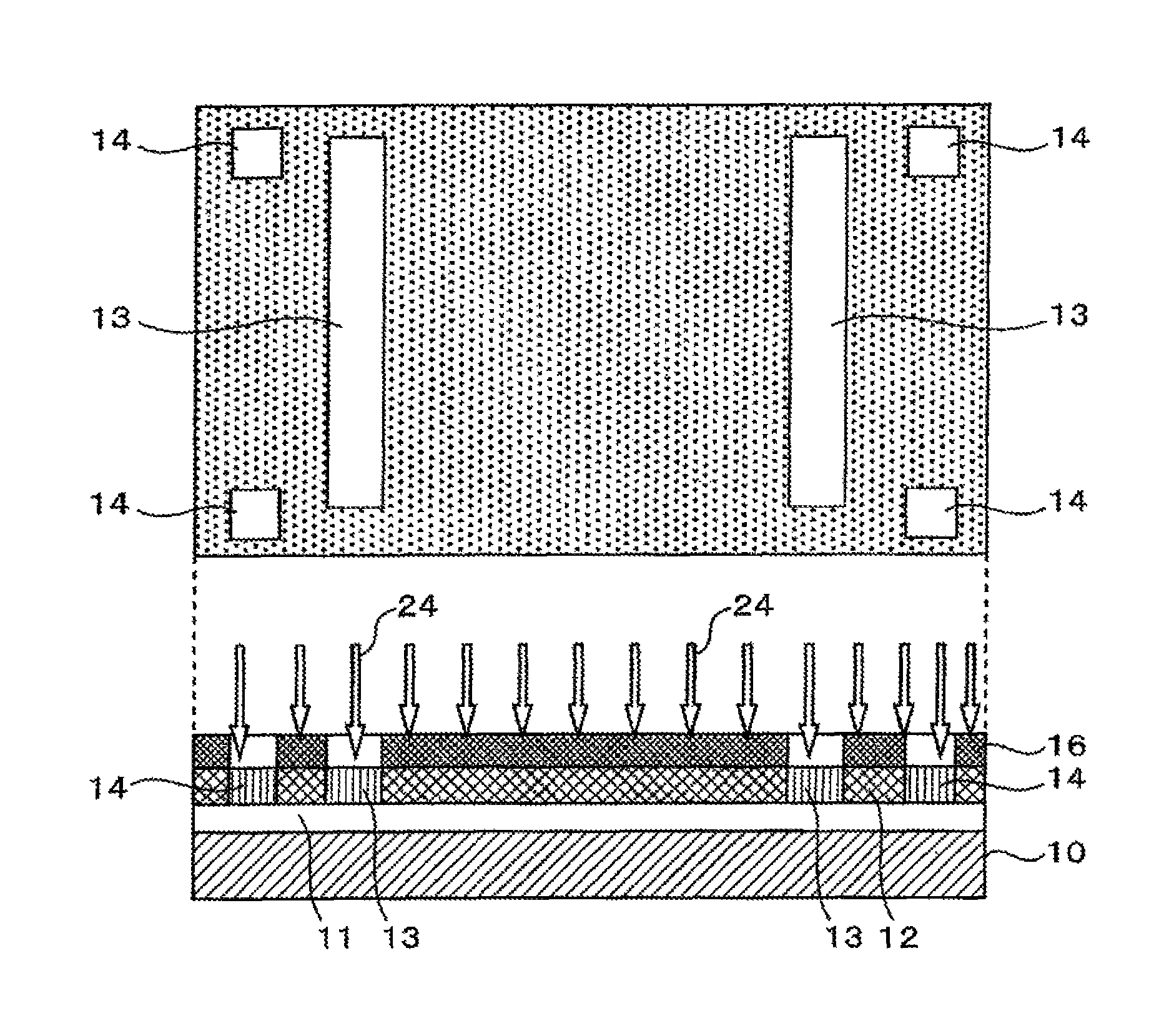
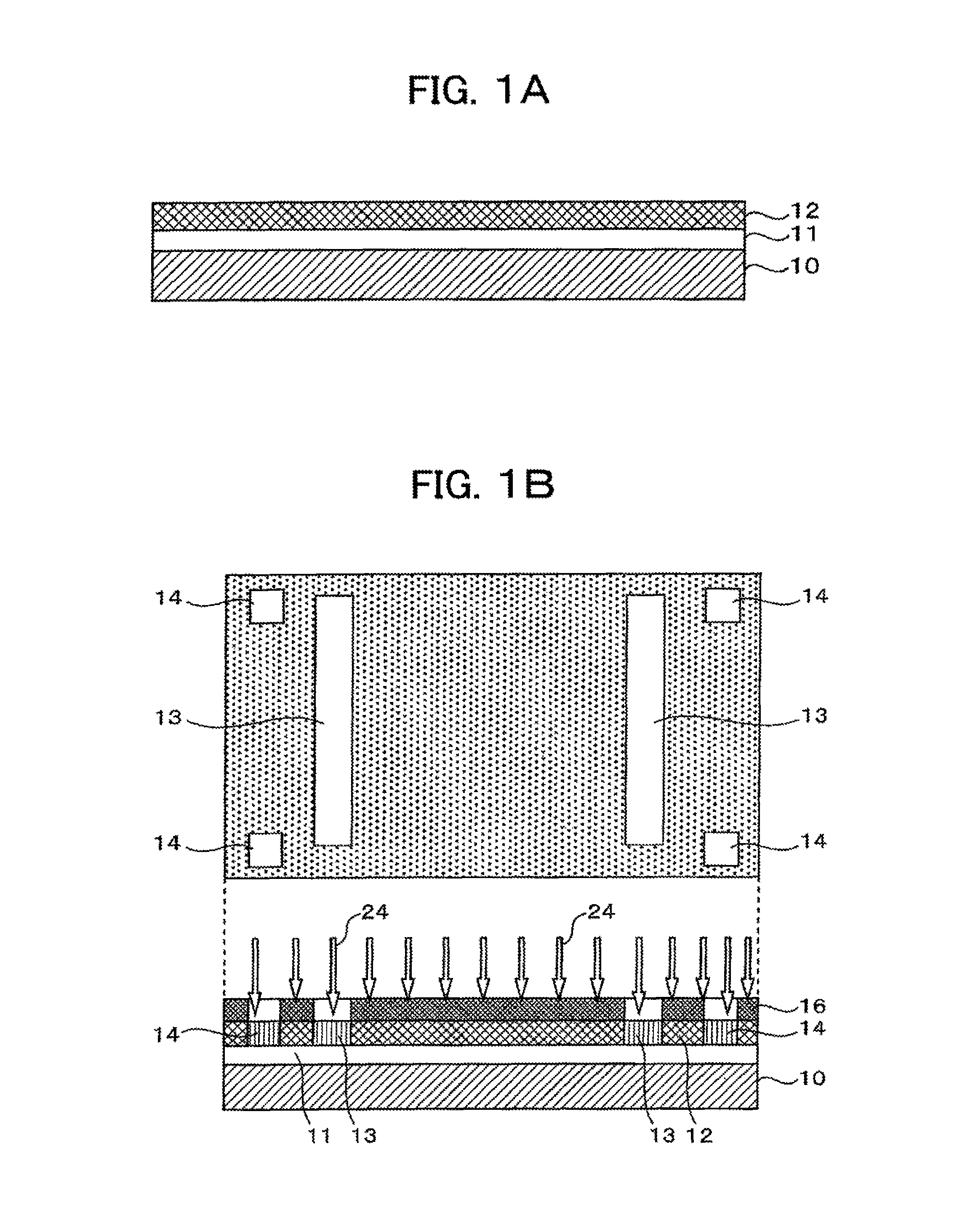
[0032]FIGS. 1A to 1G are figures for explaining a method of manufacturing an optical waveguide board that is a first embodiment of the present invention.

[0033]FIG. 1A is a figure showing a state that a clad layer 11 with thickness of approximately 30 μm is formed on a board 10, and thereon a core member 12 with a refractive index higher than that of the clad layer 11 and thickness of approximately 50 μm is formed by spin coating or lamination.

[0034]In the present embodiment, glass epoxy generally used in a printed board is used as a board material, and as materials of the clad layer 11 and the core member 12, photosensitive polymers that have absorption peaks in the ultraviolet light wavelength band, are cured by being irradiated with ultraviolet light, and can be patterned by photo-lithography are used from the aspect of simplification of a fabrication step and affinity with a printed board.

[0035]Next, as shown in FIG. 1B, by photo-lithography of irradiating ultraviolet light 24 on...

second embodiment

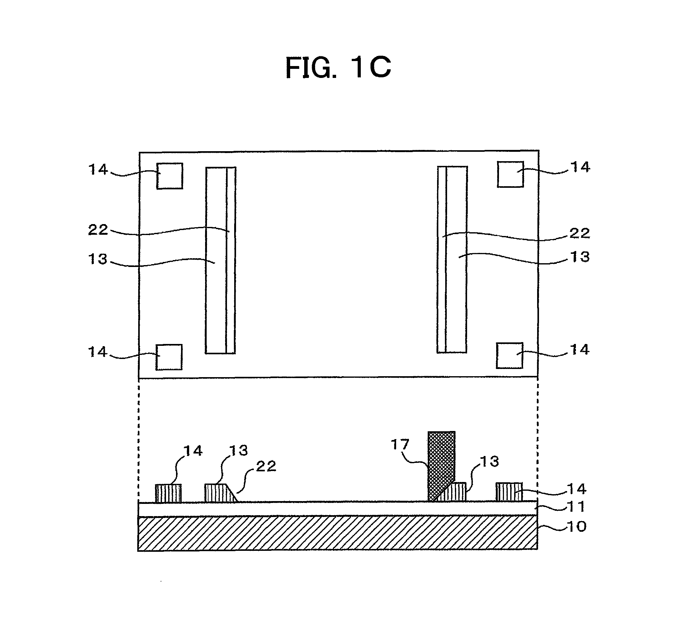
[0041]FIG. 2 is a view of the top surface and a cross section of an optical waveguide board that is a second embodiment of the present invention. Here, an example that two optical waveguide layers are laminated in the optical waveguide board of the present invention is shown.

[0042]First, the first optical waveguide layer 25 in which the mirror patterns 13, the guiding patterns 14, and the wiring core patterns 20 are respectively surrounded by the clad layer 21 is formed on the board 10 by the procedure of FIGS. 1A to 1G explained in the first embodiment. Next, guiding patterns 26 are formed on the clad layer 21 by photo-lithography simultaneously with pattern formation of the mirror members by a procedure similar to FIGS. 1A to 1B. At this time, it is possible to guide the first optical waveguide layer 25 and the patterns formed thereon relatively accurately by aligning with patterns of a photomask while observing the guiding patterns 14 in the first optical waveguide layer 25.

[0043...

third embodiment

[0046]FIG. 3 is a view of the top surface and a cross section of an optical waveguide board that is a third embodiment of the present invention. Here, an example that a laser diode and a photo diode are respectively mounted on the optical waveguide board of the present invention is shown.

[0047]As a fabrication means of this structure, first, the first optical waveguide layer 25 in which the mirror patterns 13, the guiding patterns 14, and the wiring core patterns 20 are respectively surrounded by the clad layer 21 is formed on the board 10 by the procedure of FIGS. 1A to 1G explained in the first embodiment. Next, convex shaped third guiding patterns 31 are formed on the clad layer 21 positioned on the slope parts of the mirror patterns 13 simultaneously with formation of the guiding patterns 26 by photo-lithography while observing the guiding patterns 14 in the first optical waveguide layer 25 by a procedure similar to FIGS. 1A to 1B.

[0048]Thereafter, by mating and mounting the thi...


PUM


Abstract

In the optical waveguide board, simultaneously with pattern formation of mirror members at arbitrary positions on a clad layer 11, guiding patterns 14 having convex shapes are formed respectively at arbitrary positions on peripheral parts of mirror patterns 13, and the mirror patterns 13 are worked into tapered shapes. Next, in a state that a mask member 100 having through holes at desired positions, and the guiding patterns 14 are guided by mating, a metal film is formed on surfaces of slope parts 22 of the mirror patterns and the guiding patterns 14. Furthermore, in a state that the guiding patterns 14 and the photomask 16 are guided, wiring core patterns 20 are formed on the clad layer 11 adjacent to the mirror patterns 13.

Description

TECHNICAL FIELD[0001]The present invention relates to an optical waveguide and an optical connection part provided with a guided structure in an optical waveguide board that transmits high-speed optical signals transmitted and received between chips and between boards in equipment such as a rack, and an optical-electrical hybrid board that performs bulk processing of the transmitted and received optical signals on the board, and a method of manufacturing a board using the same.BACKGROUND ART[0002]In recent years, in the information and telecommunications field, maintenance of communication traffic using optical signals has been progressed rapidly, and so far backbone-, metro-, and access-system fiber-optic networks for relatively long distance communication of several kilometers or more have been deployed. From now on, furthermore, it is effective to use optical signals for processing a large amount of data without delays in short distance rack-to-rack (several meters to several hun...

Claims


Application Information

Patent Timeline
Patent Type & Authority Patents(United States)
IPC IPC(8): G02B6/12G02B6/138G02B6/42G02B6/43
CPCG02B6/43G02B6/4249G02B6/138G02B6/4214G02B6/4224G02B6/12
Inventor MATSUOKA, YASUNOBUSUGAWARA, TOSHIKI
Owner RESONAC CORPORATION
Why Eureka
Try Eureka