Deposition substrate of deposition apparatus, method of forming layer using the same, and method of manufacturing organic light emitting diode display device

a technology of light-emitting diodes and deposition substrates, which is applied in the direction of transportation and packaging, vacuum evaporation coatings, coatings, etc., can solve the problems of difficult manufacturing of large-sized devices, limited material suitable for forming organic layers other than emitting layers, and difficult alignment between masks and subjects

Inactive Publication Date: 2015-02-10
DAWONSYS
View PDF8 Cites 2 Cited by
  • Summary
  • Abstract
  • Description
  • Claims
  • Application Information

AI Technical Summary

Benefits of technology

[0026]According to the present invention, a method of forming a layer suitable for manufacturing a large-sized device is provided.
[0027]According to the present invention, a patterning method of forming a layer during the manufacture of a device without photolithography or a separate shadow mask is provided.
[0028]Compared to a conventional layer forming method, the present method can form a layer for a very short time.

Problems solved by technology

For example, an inkjet printing method among the methods of forming a polymer or small-molecular emitting layer has disadvantages in that materials suitable for forming organic layers other than the emitting layer are limited, and a structure for inkjet printing should be formed on a substrate.
As the metal mask is increased in size, it is difficult to manufacture a large-sized device due to sagging of the metal mask.
In this case, however, due to the sagging of the mask, alignment between the mask and the subject is difficult, and thus a large-sized device is also difficult to be manufactured.

Method used


Image

  • Deposition substrate of deposition apparatus, method of forming layer using the same, and method of manufacturing organic light emitting diode display device
  • Deposition substrate of deposition apparatus, method of forming layer using the same, and method of manufacturing organic light emitting diode display device
  • Deposition substrate of deposition apparatus, method of forming layer using the same, and method of manufacturing organic light emitting diode display device

Examples


Embodiment Construction

[0037]Hereinafter, exemplary embodiments of the present invention will be described in detail. However, the present invention is not limited to the exemplary embodiments disclosed below, but can be implemented in various types. Therefore, the present exemplary embodiments are provided for complete disclosure of the present invention and to fully inform the scope of the present invention to those ordinarily skilled in the art.

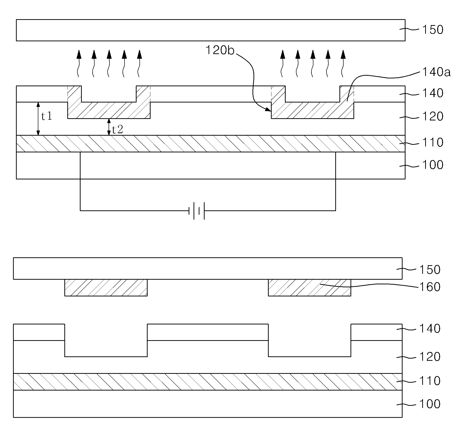
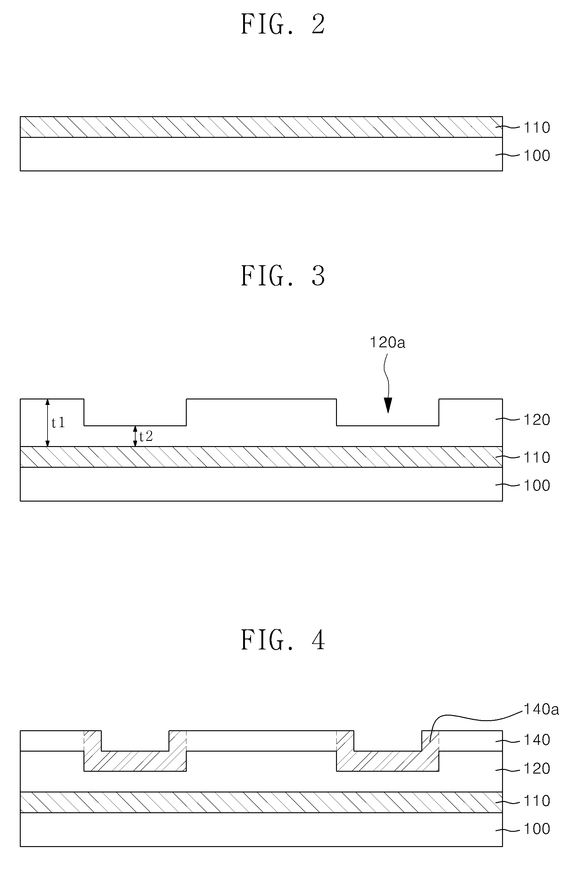
[0038]FIGS. 2 to 4 are schematic cross-sectional views of a deposition substrate of a deposition apparatus according to a first exemplary embodiment of the present invention. Here, for clarity, in the accompanying drawings, a configuration of the deposition substrate is merely illustrated, and the deposition substrate may be disposed in a vacuum chamber.

[0039]First, referring to FIG. 2, a heating conductive layer 110 for Joule heating is formed on a substrate 100 using, for example, glass, ceramic or plastic.

[0040]The heating conductive layer 110 for Joule heati...


PUM

PropertyMeasurementUnit
temperatureaaaaaaaaaa
reflectivityaaaaaaaaaa
thicknessaaaaaaaaaa

Abstract

Provided are a deposition substrate of a deposition apparatus, a method of forming a layer using the same, and a method of manufacturing an organic light emitting diode (OLED) display device. The method of forming a layer using the deposition substrate includes preparing a substrate, forming a heating conductive layer for Joule heating on the substrate, forming a first insulating layer on the heating conductive layer for Joule heating and including a groove or hole, forming a deposition material layer on a top surface of the first insulating layer having the groove or hole, and applying an electric field to the heating conductive layer for Joule heating to perform Joule-heating on the deposition material layer. Thus, the method is suitable for manufacturing a large-sized device.

Description

TECHNICAL FIELD[0001]The present invention relates to a method of forming a layer using a deposition substrate of a deposition apparatus, and more particularly, to a method of forming a layer to deposit a predetermined layer by Joule heating by applying an electric field to a conductive layer.BACKGROUND ART[0002]Among flat panel display devices, an organic light emitting diode (OLED) display device has an advantage as a moving picture display medium regardless of the size of the device due to a high response time of 1 ms or less, low power consumption, a self emission characteristic, and a wide viewing angle. The OLED display device has also attracted attention as a next-generation flat panel display device because it can be manufactured at a low temperature by a simple process based on conventional semiconductor process technology.[0003]Methods of forming a thin film of the flat panel display device or OLED display device are roughly classified into methods for a polymer device usi...

Claims


Application Information

Patent Timeline
Patent Type & Authority Patents(United States)
IPC IPC(8): H01L23/34H01L51/56B32B3/26B32B3/30C23C14/04C23C14/26H01L51/00H01L51/50
CPCH01L51/0002C23C14/04C23C14/26H01L51/0013B32B3/266B32B3/30H01L51/5012H01L51/5048Y10T428/24331Y10T428/24545Y10T428/24521H10K71/18H10K50/11H10K50/14H05B33/10C23C14/24H10K71/00H10K71/10
Inventor RO, JAE-SANGHONG, WON-EUI
Owner DAWONSYS
Why Eureka
Try Eureka