Semiconductor device and method of manufacturing semiconductor device

a semiconductor device and semiconductor technology, applied in the direction of semiconductor devices, electrical devices, transistors, etc., can solve the problems of low reliability of the semiconductor device, significant decrease in carrier mobility, and easy cause of oxygen vacancy or dangling bond defects, etc., to achieve stable electric characteristics, reduce surface roughness, and low defect density

Active Publication Date: 2015-03-24
SEMICON ENERGY LAB CO LTD
View PDF139 Cites 21 Cited by
  • Summary
  • Abstract
  • Description
  • Claims
  • Application Information

AI Technical Summary

Benefits of technology

[0008]However, in a film of an amorphous oxide semiconductor, a defect such as an oxygen vacancy or a dangling bond is easily caused. Because of such a defect, the electric conductivity or carrier density of the amorphous oxide semiconductor film is easily changed. Furthermore, such a defect causes a significant decrease in carrier mobility. Therefore, change or variation in the electric characteristics of a transistor formed using the amorphous oxide semiconductor film is remarkable, which results in low reliability of the semiconductor device.
[0009]Moreover, since the amorphous oxide semiconductor film has no crystallinity or low crystallinity, the mobility of the transistor formed using the amorphous oxide semiconductor film is low.
[0010]In view of the above problems, an object is to provide a highly reliable semiconductor device having stable electric characteristics by using an oxide semiconductor film having stable electric characteristics. Another object is to provide a semiconductor device having higher mobility by using an oxide semiconductor film having high crystallinity.
[0011]A crystalline oxide semiconductor film is formed over and in contact with an insulating film whose surface roughness is reduced, whereby the oxide semiconductor film can have high crystallinity and stable electric characteristics. Specifically, the following structure can be employed for example.
[0026]A crystalline oxide semiconductor film is formed over and in contact with an insulating film whose surface roughness is reduced, whereby the oxide semiconductor film can have low defect density and stable electric characteristics. By using such an oxide semiconductor film for a semiconductor device, a highly reliable semiconductor device having stable electric characteristics can be provided. Moreover, an oxide semiconductor film having high crystallinity can be formed; therefore, by using the oxide semiconductor film, a semiconductor device having higher mobility can be provided.

Problems solved by technology

However, in a film of an amorphous oxide semiconductor, a defect such as an oxygen vacancy or a dangling bond is easily caused.
Furthermore, such a defect causes a significant decrease in carrier mobility.
Therefore, change or variation in the electric characteristics of a transistor formed using the amorphous oxide semiconductor film is remarkable, which results in low reliability of the semiconductor device.
Moreover, since the amorphous oxide semiconductor film has no crystallinity or low crystallinity, the mobility of the transistor formed using the amorphous oxide semiconductor film is low.

Method used


Image

  • Semiconductor device and method of manufacturing semiconductor device
  • Semiconductor device and method of manufacturing semiconductor device
  • Semiconductor device and method of manufacturing semiconductor device

Examples


embodiment 1

[0047]In this embodiment, as one embodiment according to the present invention, an oxide semiconductor film that can be used for a semiconductor device and a method of forming the oxide semiconductor film will be described with reference to FIGS. 1A to 1C, FIGS. 2A to 2C, and FIGS. 3A and 3B.

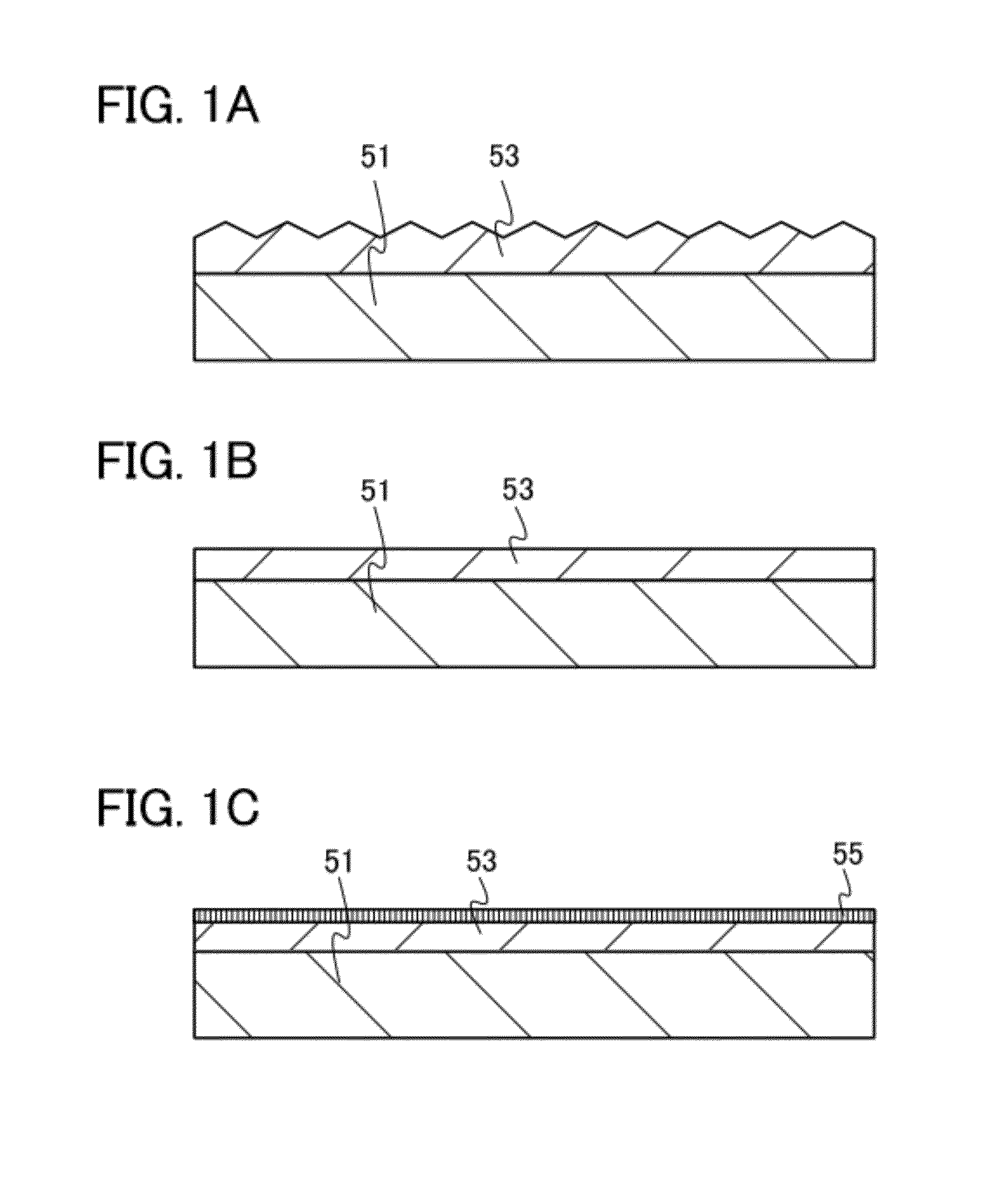
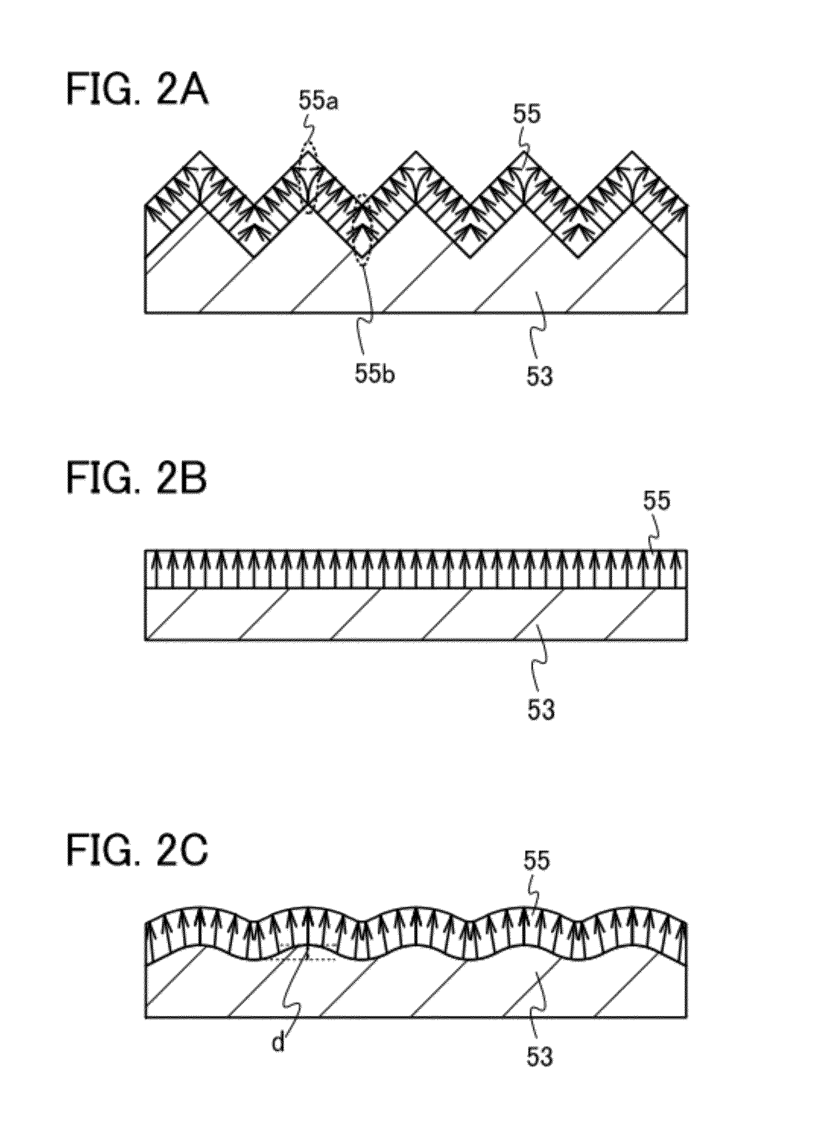
[0048]FIGS. 1A to 1C are cross-sectional views illustrating a formation process of an oxide semiconductor film that can be used for a semiconductor device. In this embodiment, as illustrated in FIG. 1C, a crystalline oxide semiconductor film 55 is formed over and in contact with an insulating film 53 which is provided over a substrate 51 and whose surface roughness is reduced.

[0049]The oxide semiconductor film 55 includes a crystalline region. The crystalline region includes a crystal whose a-b plane is substantially parallel to a surface of the insulating film 53 and whose c-axis is substantially perpendicular to the surface of the insulating film 53. That is, the oxide semiconductor film 55 in...

embodiment 2

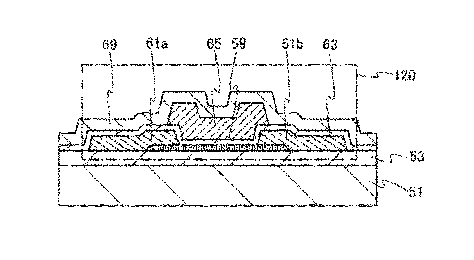
[0109]In this embodiment, as an example of a semiconductor device formed using the crystalline oxide semiconductor film described in the above embodiment, a transistor formed using the oxide semiconductor film and a method of manufacturing the transistor will be described with reference to FIGS. 4A to 4D and FIGS. 5A to 5C. FIGS. 4A to 4D are cross-sectional views illustrating a manufacturing process of a transistor 120 having a top-gate structure which is one embodiment of a structure of a semiconductor device.

[0110]First, as illustrated in FIG. 4A, the oxide semiconductor film 55 is formed over and in contact with the insulating film 53 provided over the substrate 51, by the method described in the above embodiment. Then, the oxide semiconductor film 55 is selectively etched with the use of a mask, so that an oxide semiconductor film 59 is formed as illustrated in FIG. 4B. After that, the mask is removed.

[0111]The mask used in the etching of the oxide semiconductor film 55 can be ...

embodiment 3

[0136]In this embodiment, as an example of a semiconductor device formed by the method of manufacturing a semiconductor device described in the above embodiment, a storage medium (memory element) will be described. In this embodiment, a transistor formed using an oxide semiconductor by the method of manufacturing a semiconductor device described in the above embodiment, and a transistor formed using a material other than an oxide semiconductor are formed over one substrate.

[0137]FIGS. 6A to 6C illustrate an example of a structure of a semiconductor device. FIG. 6A illustrates a cross section of the semiconductor device, and FIG. 6B illustrates a plan view of the semiconductor device. Here, FIG. 6A illustrates a cross section taken along line C1-C2 and line D1-D2 in FIG. 6B. In addition, FIG. 6C is an example of a diagram of a circuit using the semiconductor device as a memory element. In the semiconductor device illustrated in FIGS. 6A and 6B, a transistor 500 formed using a first s...


PUM


Abstract

An object is to provide a highly reliable semiconductor device having stable electric characteristics by using an oxide semiconductor film having stable electric characteristics. Another object is to provide a semiconductor device having higher mobility by using an oxide semiconductor film having high crystallinity. A crystalline oxide semiconductor film is formed over and in contact with an insulating film whose surface roughness is reduced, whereby the oxide semiconductor film can have stable electric characteristics. Accordingly, the highly reliable semiconductor device having stable electric characteristics can be provided. Further, the semiconductor device having higher mobility can be provided.

Description

BACKGROUND OF THE INVENTION[0001]1. Field of the Invention[0002]The present invention relates to a semiconductor device formed using an oxide semiconductor film and a method of manufacturing the semiconductor device.[0003]In this specification, a semiconductor device means all types of devices which can function by utilizing semiconductor characteristics, and an electro-optical device, a semiconductor circuit, and an electronic device are all semiconductor devices.[0004]2. Description of the Related Art[0005]In recent years, a technique by which a semiconductor device typified by a transistor is manufactured using a semiconductor thin film formed over a substrate having an insulating surface has been attracting attention. Such a semiconductor device is applied to a wide range of electronic devices such as an integrated circuit (IC) or an image display device (display device). As a material of a semiconductor thin film that can be applied to such a semiconductor device typified by a ...

Claims


Application Information

Patent Timeline
Patent Type & Authority Patents(United States)
IPC IPC(8): H01L29/786H01L21/36H01L29/423H01L29/66
CPCH01L29/7869H01L29/42384H01L29/66742H01L29/78603H01L29/04H01L29/06H01L29/0684H01L29/66409H01L29/786H01L29/66969H01L27/105H01L21/0214H01L21/02164H01L21/02238H01L21/02255H01L21/02565H01L21/44H01L21/47573H01L21/477H01L29/045H01L29/24
Inventor HONDA, TATSUYAOMATA, TAKATSUGUNONAKA, YUSUKE
Owner SEMICON ENERGY LAB CO LTD
Why Eureka
Try Eureka