Mask blank, transfer mask, and method of manufacturing a transfer mask
a technology of mask blanks and masks, applied in the field of mask blanks, transfer masks, and methods of manufacturing transfer masks, can solve the problems of black defect correction by such a physical treatment that takes a long time, and the problem of ga stain remaining on qz substrates
- Summary
- Abstract
- Description
- Claims
- Application Information
AI Technical Summary
Benefits of technology
Problems solved by technology
Method used
Image

Examples
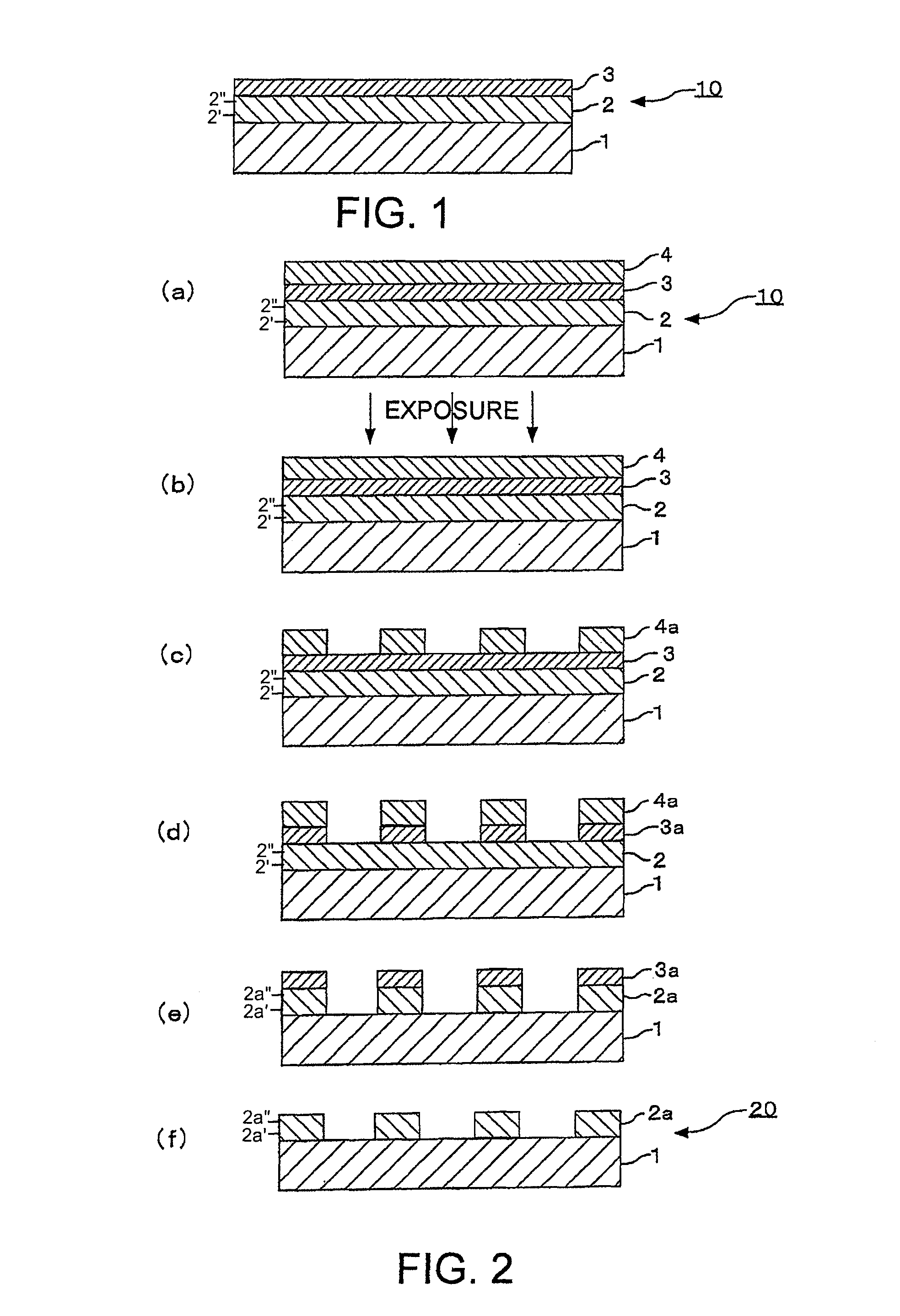
example 1
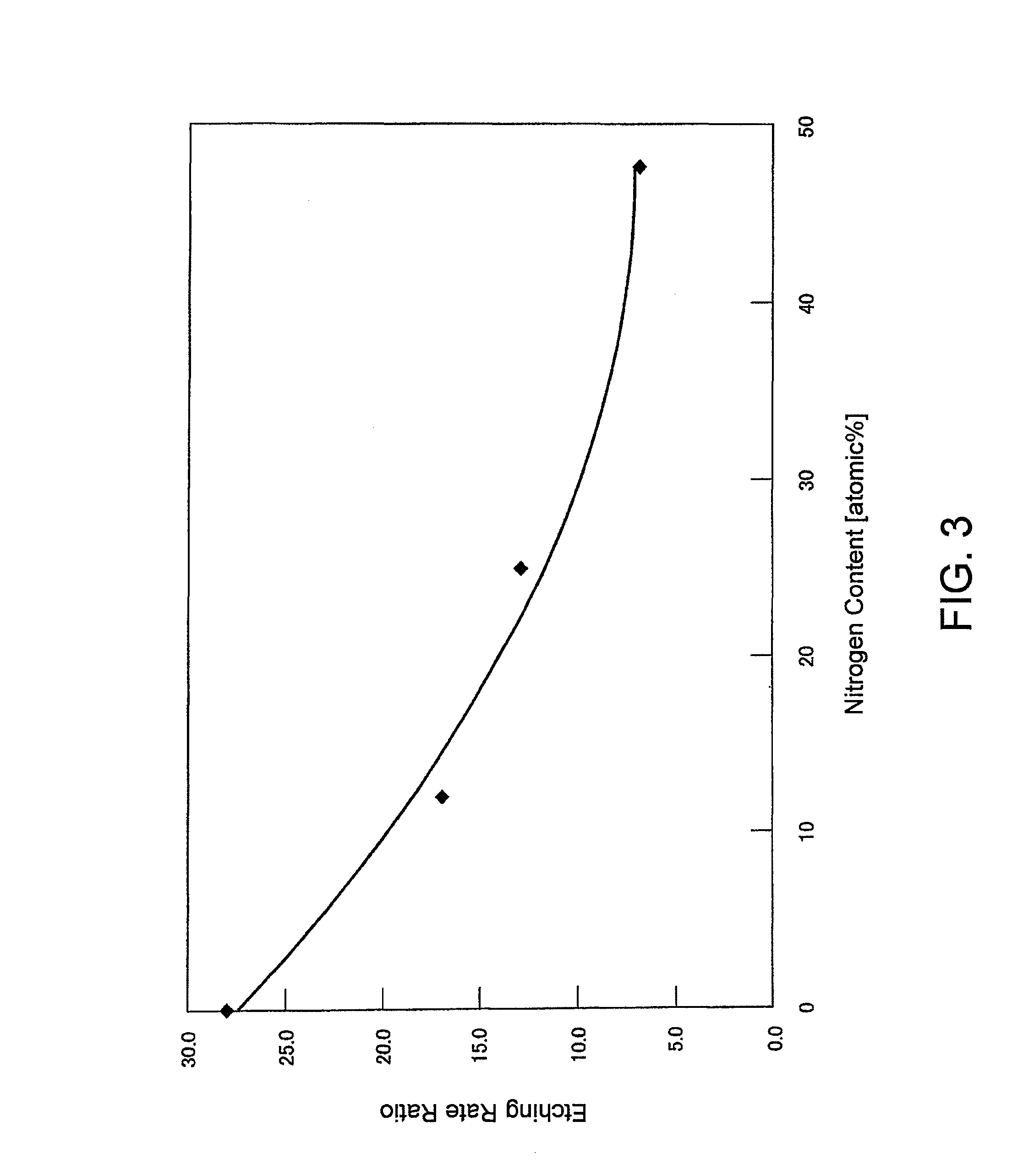
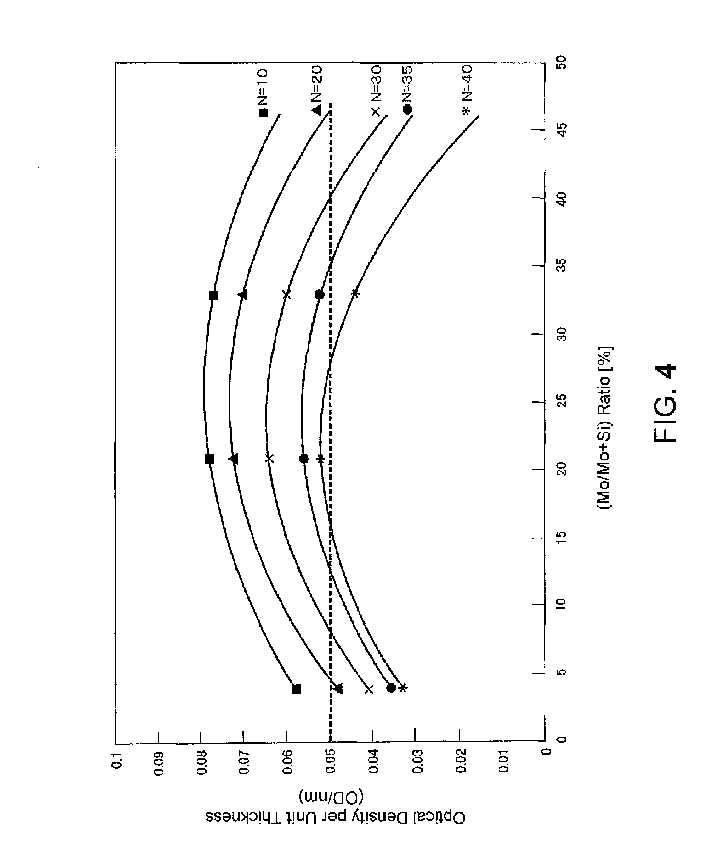
[0099]In a single-wafer sputtering apparatus, using a mixed target of molybdenum (Mo) and silicon (Si) (at % ratio Mo:Si=21:79) as a sputtering target, reactive sputtering (DC sputtering) was carried out by setting the power of a DC power supply to 2.1 kW in a mixed gas atmosphere of argon and nitrogen (gas pressure 0.07 Pa, gas flow rate ratio Ar:N2=25:28), thereby forming a MoSiN film (lower layer (light-shielding layer)) to a thickness of 50 nm on a transparent substrate 1 made of synthetic quartz glass. Then, using a Mo / Si target (at % ratio Mo:Si=4:96), reactive sputtering (DC sputtering) was carried out by setting the power of a DC power supply to 3.0 kW in a mixed gas atmosphere of argon, oxygen, nitrogen, and helium (gas pressure 0.1 Pa, gas flow rate ratio Ar:O2:N2:He=6:3:11:17), thereby forming a MoSiON film (upper layer (front-surface antireflection layer)) to a thickness of 10 nm. In this manner, there was formed a light-shielding film 2 (total thickness 60 nm) for ArF e...
example 2
[0111]In a single-wafer sputtering apparatus, using a mixed target of molybdenum (Mo) and silicon (Si) (at % ratio Mo:Si=21:79) as a sputtering target, reactive sputtering (DC sputtering) was carried out by setting the power of a DC power supply to 2.1 kW in a mixed gas atmosphere of argon, methane, and nitrogen (gas pressure 0.07 Pa, gas flow rate ratio Ar+CH4 (8%):N2=25:28), thereby forming a MoSiNCH film (lower layer (light-shielding layer)) to a thickness of 50 nm on a transparent substrate 1 made of synthetic quartz glass. Then, using a Mo / Si target (at % ratio Mo:Si=4:96), reactive sputtering (DC sputtering) was carried out by setting the power of a DC power supply to 3.0 kW in a mixed gas atmosphere of argon, oxygen, nitrogen, and helium (gas pressure 0.1 Pa, gas flow rate ratio Ar:O2:N2:He=6:3:11:17), thereby forming a MoSiON film (upper layer (front-surface antireflection layer)) to a thickness of 10 nm. In this manner, there was formed a light-shielding film 2 (total thick...
example 3
[0117]In a single-wafer sputtering apparatus, using a mixed target of molybdenum (Mo) and silicon (Si) (at % ratio Mo:Si=21:79) as a sputtering target, reactive sputtering (DC sputtering) was carried out by setting the power of a DC power supply to 2.1 kW in a mixed gas atmosphere of argon and nitrogen (gas pressure 0.07 Pa, gas flow rate ratio Ar:N2=25:15), thereby forming a MoSiN film (lower layer (light-shielding layer)) to a thickness of 49 nm on a transparent substrate 1 made of synthetic quartz glass. Then, using a Mo / Si target (at % ratio Mo:Si=4:96), reactive sputtering (DC sputtering) was carried out by setting the power of a DC power supply to 3.0 kW in a mixed gas atmosphere of argon, oxygen, nitrogen, and helium (gas pressure 0.1 Pa, gas flow rate ratio Ar:O2:N2:He=6:3:11:17), thereby forming a MoSiON film (upper layer (front-surface antireflection layer)) to a thickness of 10 nm. In this manner, there was formed a light-shielding film 2 (total thickness 59 nm) for ArF e...
PUM
| Property | Measurement | Unit |
|---|---|---|
| thickness | aaaaa | aaaaa |
| thickness | aaaaa | aaaaa |
| wavelength | aaaaa | aaaaa |
Abstract
Description
Claims
Application Information
 - R&D
- Intellectual Property
- Life Sciences
- Materials
- Tech Scout
- Unparalleled Data Quality
- Higher Quality Content
- 60% Fewer Hallucinations
Browse by: Latest US Patents, China's latest patents, Technical Efficacy Thesaurus, Application Domain, Technology Topic, Popular Technical Reports.
© 2025 PatSnap. All rights reserved.Legal|Privacy policy|Modern Slavery Act Transparency Statement|Sitemap|About US| Contact US: help@patsnap.com